Double Peak Phenomenon with Op-Amp Transimpedance circuit

Thread Starter

jsyschan

Joined Apr 28, 2012
12
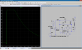
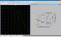
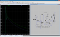
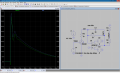
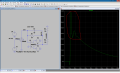
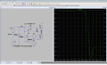
I'm trying to understand why a transimpedance amplifier behaves the way it does. I'm running a simulation of a transimpedance amplifier circuit using the AD8014 and a silicon photomultiplier. You can see the circuit in my attachments below. The silicon photomultiplier is being triggered by a 5 volt pulse source. The first image shows the transient response, with the output signal at LOAD1 and the double peak occurring in red. The second image shows the frequency response of the circuit at LOAD1. I don't understand why the double-peak is occurring, and frequency response doesn't tell me much, though it is strange that it doesn't start out over 0 dB. I tried using other amplifiers, and with a low valued feedback resistor, I also see the double peak phenomenon. Why does this occur, and what can I do about it?

EDIT: To give a little more detail, I'm trying to amplify the signal coming from the SiPM, convert current to a voltage signal quickly and without saturating/becoming clipped. I thought to reduce the feedback resistance to get a faster response time, but it seems to make it worse.
 

Attachments

ebp

Joined Feb 8, 2018
2,332
It would be helpful if your simulation waveforms included the actual current from the photomultiplier, so we don't have to guess at the mysteries of the model for it.

Many high speed current feedback amps are optimized for a relatively narrow range of feedback resistance, often from a few hundred ohms to one or two kilohms. If you really need extremely low feedback resistance because of high output from the photomultiplier and therefore require very low gain, I would suggest contacting AD for some advice.

It looks to me like the waveform is severe high-frequency peaking with ring-down. How was the gain-phase plot produced?
 

Thread Starter

jsyschan

Joined Apr 28, 2012
12
It would be helpful if your simulation waveforms included the actual current from the photomultiplier, so we don't have to guess at the mysteries of the model for it.

Many high speed current feedback amps are optimized for a relatively narrow range of feedback resistance, often from a few hundred ohms to one or two kilohms. If you really need extremely low feedback resistance because of high output from the photomultiplier and therefore require very low gain, I would suggest contacting AD for some advice.

It looks to me like the waveform is severe high-frequency peaking with ring-down. How was the gain-phase plot produced?

Thanks for your reply. Sorry about the vague description. Please let me give a bit more detail about my circuit. For our SiPM, I'm using the MicroFJ-60035-TSV SiPM by SensL. We previously used the TI OPA656 for our op-amp, but the signal was too slow. With a feedback resistor of 25 ohms and a feedback capacitor of 3 pF, we got good speeds with the OPA656, around 10 ns rise time, but the output voltage was very low. I figured that I could try to replace the OPA656 with something faster, so I looked at other op-amps with faster slew rates, thus the AD8014. I figured that with a faster slew rate, I could increase the gain a bit more and still achieve the same speeds. However, my team found that with the AD8014, the output saturates/clips. You can see it in the attached image; with the AD8014, at a 100 ohm feedback resistance, the output clipped after a certain point. My team wanted a nice peak, so I reduced the gain by reducing the feedback resistance, but I found that a smaller feedback resistance resulted in this double peak phenomenon. The SiPM is rated for 15 mA max, so I'm not necessarily looking for a low feedback resistance, just trying to get a fast, clean output peak.

In regards to my simulation, the gain-phase plot was produced by performing an AC analysis using a voltage source. I received word that my method was wrong, so I have attached a new image showing my new AC analysis. This was performed by using an AC current source to simulate the current draw from the SiPM when active.
 

Attachments

ebp

Joined Feb 8, 2018
2,332
Do remember that this is a current feedback amplifier, and is quite different from a voltage feedback amp like the OPA656.

The clipping at 1 volt output on ±5 V supplies seems odd. It is heavily loaded (50 ohms - feedback in parallel with output), but it should do better than 1 volt. I would try a couple of simulation variations - increase the output load resistance and try unbalanced supplies, such as +10 V and -2 V. The behavior should at least be different. Again, 100 ohms is well below the minimum feedback resistance shown in Table II of the datasheet.

What happens if you vary the value of the feedback capacitor? At high frequency you are reducing the feedback impedance even further.
What happens if you disconnect the photomultiplier when doing the gain-phase plot? What do you know about the capacitance of the multiplier at nearly zero bias voltage? I suspect that horrible behavior at the "end" is due to capacitance. Current feedback amps are extremely sensitive to capacitance at the [EDIT - correction: was NII] inverting input.

I'd still like to the the multiplier current on the sim plot so it is possible to try to relate the amp output to the actual current input.

Doesn't the photomultiplier manufacturer have a recommendation for an amplifier?
 
Last edited:

RichardO

Joined May 4, 2013
2,270
Current feedback amps are extremely sensitive to capacitance at the NII.
Current feedback op-amps are picky beasts. They also dislike capacitance across the feedback resistor. In addition, the feedback resistor sets the bandwidth. Too small a value gives overshoot on the output, for instance.

Another thing... the PMT might not like to see the relatively large input bias current of the AD8014. This is much, much higher bias current than the ADA656.

And, finally, when you actually build the circuit it can act very different than the simulation. We are talking about very high frequencies and currents here.

For instance as @ebp said the inputs of high speed op-amps are sensitive to capacitance. Even a ground plane under the input pins can cause problems.

Of course, you need very good power supply bypassing to a good ground plane. Both ceramic SMD caps right next to the power pins as well as larger bulk bypass caps near by.
 

Bordodynov

Joined May 20, 2015
3,430
See
I do not have the parameters of your photomultiplier and I applied the avalanche photodiode. With this photodiode, the multiplication factor changes as the voltage increases (see the table at the top of the diagram).2018-04-02_15-25-48.png I showed how the output signal changes when the bias voltage changes. Your resistor ratings for the transimpedance amplifier are meaningless!
 

Thread Starter

jsyschan

Joined Apr 28, 2012
12
Do remember that this is a current feedback amplifier, and is quite different from a voltage feedback amp like the OPA656.

The clipping at 1 volt output on ±5 V supplies seems odd. It is heavily loaded (50 ohms - feedback in parallel with output), but it should do better than 1 volt. I would try a couple of simulation variations - increase the output load resistance and try unbalanced supplies, such as +10 V and -2 V. The behavior should at least be different. Again, 100 ohms is well below the minimum feedback resistance shown in Table II of the datasheet.

What happens if you vary the value of the feedback capacitor? At high frequency you are reducing the feedback impedance even further.
What happens if you disconnect the photomultiplier when doing the gain-phase plot? What do you know about the capacitance of the multiplier at nearly zero bias voltage? I suspect that horrible behavior at the "end" is due to capacitance. Current feedback amps are extremely sensitive to capacitance at the NII.

I'd still like to the the multiplier current on the sim plot so it is possible to try to relate the amp output to the actual current input.

Doesn't the photomultiplier manufacturer have a recommendation for an amplifier?
Thanks for your reply. Sorry for not showing it before. My SiPM component can't be observed directly as it's a custom component, so I just placed a very tiny resistance in series with it in order to gauge the current through it. I've attached some images showing the transient analysis and AC analysis of the supposed current to the SiPM. No current goes to the voltage trigger. I ran analysis with the resistance placed in front and behind the SiPM. The transient results seem to be the same, though there is a little noise in the AC analysis. I hope that this helps.

My choice of 50 ohms for the load was based on what the measured load is. The output of the circuit coming from R2 is going to an oscilloscope, which is seen as a 50 ohm load. That's how my team is measuring it, so that's how I'm trying to simulate it. Increasing the capacitance seems to decrease the output voltage magnitude as seen at 132 MHz, but it doesn't really seem to have much of an effect on the circuit. This is just based on short tests, so I'll run it again to check.

There is a recommended amplifier for the circuit, the OPA656, and it was suggested to use a 3 pF feedback capacitor and a 470 ohm feedback resistor. However, my team found it to be too slow, so I tried reducing the feedback resistance. It gave us faster times, but the output was very small, so we had to use an external amplifier to compensate for the loss in gain. Thus, I tried to find op-amps with faster slew rates which matched the form-factor of the OPA656 and can use the same power supplies, which lead me to the AD8014.
 

Attachments

Thread Starter

jsyschan

Joined Apr 28, 2012
12
See
I do not have the parameters of your photomultiplier and I applied the avalanche photodiode. With this photodiode, the multiplication factor changes as the voltage increases (see the table at the top of the diagram).View attachment 149596 I showed how the output signal changes when the bias voltage changes. Your resistor ratings for the transimpedance amplifier are meaningless!
Thanks for your reply. My photomultiplier is the SensL MicroFJ-60035-TSV SiPM. According to the manufacturer, their SPICE model is already properly biased, so I don't need to add a voltage bias for the SiPM in my model. When I tried to do so, the output was vastly different than what was measured, both with their model and the actual tests that my team performed, so there's no need to bias it in simulation, though I'm aware that the results will vary based on the bias voltage. My team is biasing it at -30 volts, with the bias being applied at the anode.
 

Bordodynov

Joined May 20, 2015
3,430
Strange attachment to the value of 3 pF. Usually a parasitic capacitance of the feedback resistor (~ 0.1pf) is sufficient. If you tell me what the capacitance of your photodiode is, I will calculate the minimum, necessary capacity of feedback. The feedback capacity degrades the dynamic parameters. For a larger transmission factor and an improvement in the signal-to-noise ratio, it is necessary to increase the value of the feedback resistor. You first destroy everything, and then put an additional amplifier!
 

Thread Starter

jsyschan

Joined Apr 28, 2012
12
Strange attachment to the value of 3 pF. Usually a parasitic capacitance of the feedback resistor (~ 0.1pf) is sufficient. If you tell me what the capacitance of your photodiode is, I will calculate the minimum, necessary capacity of feedback. The feedback capacity degrades the dynamic parameters. For a larger transmission factor and an improvement in the signal-to-noise ratio, it is necessary to increase the value of the feedback resistor. You first destroy everything, and then put an additional amplifier!
I'm approximating the parasitic capacitance of the SiPM to be 400 pF at the cathode based on reports by the manufacturer. They gave it as 4 nF on the datasheet, but that's at the anode output. I had to approximate the cathode capacitance based on other papers by the manufacturer. The 3 pF feedback capacitance was the value recommended by the manufacturer in their proposed transimpedance amplifier circuit.
 

Thread Starter

jsyschan

Joined Apr 28, 2012
12
Current feedback op-amps are picky beasts. They also dislike capacitance across the feedback resistor. In addition, the feedback resistor sets the bandwidth. Too small a value gives overshoot on the output, for instance.

Another thing... the PMT might not like to see the relatively large input bias current of the AD8014. This is much, much higher bias current than the ADA656.

And, finally, when you actually build the circuit it can act very different than the simulation. We are talking about very high frequencies and currents here.

For instance as @ebp said the inputs of high speed op-amps are sensitive to capacitance. Even a ground plane under the input pins can cause problems.

Of course, you need very good power supply bypassing to a good ground plane. Both ceramic SMD caps right next to the power pins as well as larger bulk bypass caps near by.
Thanks for your reply. Perhaps that's what I'm seeing, overshoot due to the low resistance. I thought that the resistor set the gain while the capacitance and resistance together set the bandwidth by moving the pole. With such a large input offset voltage/input bias current compared to the OPA656, that would reduce the output voltage, but how does it contribute to the ringing? Also, if you don't mind me asking, how do the feedback components affect the bandwidth of the op-amp?
 

RichardO

Joined May 4, 2013
2,270
Thanks for your reply. Perhaps that's what I'm seeing, overshoot due to the low resistance. I thought that the resistor set the gain while the capacitance and resistance together set the bandwidth by moving the pole. With such a large input offset voltage/input bias current compared to the OPA656, that would reduce the output voltage, but how does it contribute to the ringing? Also, if you don't mind me asking, how do the feedback components affect the bandwidth of the op-amp?
What you say about the feedback resistance and capacitance setting the bandwidth is true for a voltage feedback op-amp. It is not true for an current feedback op-amp.

Look at figure 7 in the AD8014 data sheet. You will see that the frequency response is flat with a 1K ohm feedback resistor and 1.5dB of peaking with a 300 ohm resistor. Your 50 ohm resistor is not even on the graph. :eek:

Bottom line... You can't just swap back and forth between voltage feedback op-amps and current feedback op-amps without making changes to the circuit.
 

Thread Starter

jsyschan

Joined Apr 28, 2012
12
What you say about the feedback resistance and capacitance setting the bandwidth is true for a voltage feedback op-amp. It is not true for an current feedback op-amp.

Look at figure 7 in the AD8014 data sheet. You will see that the frequency response is flat with a 1K ohm feedback resistor and 1.5dB of peaking with a 300 ohm resistor. Your 50 ohm resistor is not even on the graph. :eek:

Bottom line... You can't just swap back and forth between voltage feedback op-amps and current feedback op-amps without making changes to the circuit.
Thanks for your reply. To be honest, I wasn't aware of this. I thought that despite their differences, both amplifiers would work the same way. Looks like I'll have to do some more research then to see if using a CFA is feasible somehow. If not, I'll remember to go back to VFAs.
 
Last edited:
Top