Facebook
 Google
 GitHub
 Linkedin
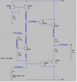
In this procedure it's not considered the signal swing. Shouldn't I check that the maximum voltage swing is allowed in every stage?The quiescent current of the input stage is select based on Q8 base current (VAS stage - Voltage Amplifier Stage).
Since the input and the VAS work in class A we need to choose I_input_stage >> I_vas.
But in this case, I just pick a nice round number IcQ10 = 1mA.
In the mentioned link:
https://forum.allaboutcircuits.com/...ign-basic-questions.104719/page-6#post-804580
A formula is used to find the current in differential branches:
ICQ1 = 10 * ICQ3/Hfe_min = 10 * 20mA/100 = 2mA
Is even this formula a rule of thumb formula?
Last edited:
.PNG")
.PNG")