Switching function of both BJT and Mosfet

Thread Starter

Josh1233

Joined Aug 25, 2022
9
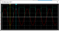
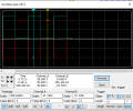
Both of this graph show mosfet and but in switching mode
As i look at the graph below I notice for mosfet the drain source amplitude is higher than the gate voltage amplitude . However , bjt , collector voltage amplitude is only reach at the same amplitude of base voltage amplitude. From this graph it that mean mosfet amplify as it switching ( which I believe it should not be)? could you guy explain why the Drain source voltage of mosfet higher than input gate voltage? Furthermore why bjt don’t act the same?


57065F9B-1116-491A-90F9-83CAA4B536C8.jpeg 514C106E-6043-4928-B006-051A762E17E3.jpeg
 

MrChips

Joined Oct 2, 2009
30,701
Welcome to AAC!

There is no voltage scale shown in the diagrams. Hence there is no indication of the voltages required to turn on the BJT or MOSFET.

Typically, a BJT has a VBE turn on voltage of 0.6-0.7V.
You need to examine the datasheet of each MOSFET to determine the VGS switching threshold.
 

Thread Starter

Josh1233

Joined Aug 25, 2022
9
Welcome to AAC!

There is no voltage scale shown in the diagrams. Hence there is no indication of the voltages required to turn on the BJT or MOSFET.

Typically, a BJT has a Vbe turn on voltage of 0.6-0.7V.
You need to examine the datasheet of each MOSFET to determine the Vgs switching threshold.

Hi ,

I had measured power mosfet as a switch . The yellow wave is PWM which an input to the gate . The blue wave is output Voltage between Drain and Source . What i got is the amplitude of voltage between Drain and Source is 250 V which much higher than the input. I dont understand why the voltage between Drain and Source so high compare to input. Is that mean i measured the voltage wrong?


IMG_0035.jpg
 

MrChips

Joined Oct 2, 2009
30,701
The MOSFET VDS voltage is a function of the supply voltage and the circuit configuration.
Reduce the supply voltage to 10V and you will see VDS being reduced accordingly.
 

crutschow

Joined Mar 14, 2008
34,280
The drain voltage when the MOSFET is off (Vgs below its threshold) is equal to the drain supply voltage.
Why do you think that's unusual?

When Vgs is sufficiently above the Vgs threshold then the MOSFET is fully on, and Vds equals the drain current times the MOSFET ON-resistance.

You seem to have a fundamental misunderstanding of how MOSFETs work.
Suggest you read a tutorial on that.
 

Thread Starter

Josh1233

Joined Aug 25, 2022
9
The MOSFET VDS voltage is a function of the supply voltage and the circuit configuration.
Reduce the supply voltage to 10V and you will see VDS being reduced accordingly.
For the graph I measured , Do you mean as I increase duty cycle or amplitude of input or frequency of input the output V(DS) will increased ? Because when i use multism simulation to compare with what i measured . The output V(DS) seem to be constant even i change my duty cycle , amplitude or frequency. The output always constant at 24V.

1661437787923.png

Amplitude at 10 peak to peak and duty cycle at 51% frequency 1kHz

1661437838435.png


Amplitude at 43 peak to peak and duty cycle at 86% frequency 1kHz
1661437953264.png
 

Attachments

MrChips

Joined Oct 2, 2009
30,701
The BJT or MOSFET is behaving as a closed switch when operating in saturation mode. The signal amplitude will be close to the supply voltage when in the off state.

Assuming that you do not exceed the max frequency of the MOSFET and its circuit, the frequency and duty cycle do not affect the signal amplitude.
 

Thread Starter

Josh1233

Joined Aug 25, 2022
9
The BJT or MOSFET is behaving as a closed switch when operating in saturation mode. The signal amplitude will be close to the supply voltage when in the off state.

Assuming that you do not exceed the max frequency of the MOSFET and its circuit, the frequency and duty cycle do not affect the signal amplitude.
Oh , i understand the concept now. But what i confusing is my reality measurement. The graph that i show you at my second reply . My reality circuit also set the DC supply to be 24V . The V(DS) seem to be 250 peak to peak according to the graph when Mosfet at off state. I expect it will be around 24 V supply [should be 48 peak to peak. ]Do it mean there is an error in my reality circuit?

Legend
Blue wave : V(DS)
Yellow : PWM input to gate terminal
 

Attachments

MrChips

Joined Oct 2, 2009
30,701
If your supply voltage is 24V then the output of the switched MOSFET will be from 0V to 24V, not 48V peak-to-peak.
 
Top