SPICE Simulation is Great; Circuit Implementation Fails!

Thread Starter

phillipsoasis

Joined Aug 22, 2022
170
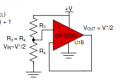
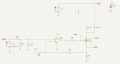
I have a simple DAC driving a MOSFET for a voltage controlled current source (see attached KiCad 7 files) driving two loads - a light bulb (9R) or an igniter (~0.4R). The simulation does what I want for both the bulb and the igniter. When the bulb is in use, the current is limited to ~1A by the value programmed into the DAC. When the igniter is used, the DAC is at maximum. When I built the circuit, it fails miserably. No matter what values I program into the DAC, the MOSFET is full on pulling ~ 1.24.

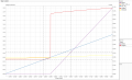
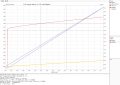
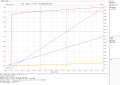
The simulation uses a voltage source to simulate the DAC. I just ramp up the voltage from 0 to 3.3V for the Rigniter load in the simulation to see what is happening. For the bulb, I ramp the voltage from 0 to 1.2V to get ~1A to light the bulb.

In the real circuit, the DAC appears to be working. The voltage increases as expected as I increase the values programmed into the DAC from a Raspberry Pi through the SDI bus. I checked the SDI bus with a logic analyzer, and the values/timing coming across the wires are correct.

The TLV2462 may be the errant child. If I pull the chip, the V- input is at the correct bias voltage. If I put the chip back in, V- jumps to 1.192V without the 15V supply turned on. With the 15V supply on, V- signal is sitting at 1.22V. The 15V power supply says it is delivering 18 W. The DAC output when programmed for 0V is 1.2 mV, as expected. But the V+ pin is at 0.733V. I have created perpetual motion!

Is the TLV2462 dead? I did not "tie off" the other op amp in the package - could that be the problem? Am I missing something fundamental in the circuit operation?

Thanks!
 

Attachments

WBahn

Joined Mar 31, 2012
32,702
Why are you tying the left side of R106 to 3.3 V? Unless you have some specific reason for doing this, it is probably going to cause problems (which may or may not be big enough to be an issue).

You definitely want to properly connect the unused opamp in the package to prevent it from either oscillating or going into some kind of high-current draw mode. While tying one input to one supply and the other input to the other supply is likely sufficient, some opamps do not like to have their inputs be outside their input voltage range, which does not always include the rails. A common way of dealing with this is to put something like three 10 kΩ (or higher, depending on the input bias current of the opamp) in series between the supply rails and connecting one junction to one input and the other junction to the other input. This puts each input 1/3 of they way from the rail, which is almost always well within the input voltage range, and ensures enough voltage difference at the input to overdrive the amp and force it to rail the output one way or the other (leave the output unconnected).
 

Thread Starter

phillipsoasis

Joined Aug 22, 2022
170
Why are you tying the left side of R106 to 3.3 V? Unless you have some specific reason for doing this, it is probably going to cause problems (which may or may not be big enough to be an issue).

You definitely want to properly connect the unused opamp in the package to prevent it from either oscillating or going into some kind of high-current draw mode. While tying one input to one supply and the other input to the other supply is likely sufficient, some opamps do not like to have their inputs be outside their input voltage range, which does not always include the rails. A common way of dealing with this is to put something like three 10 kΩ (or higher, depending on the input bias current of the opamp) in series between the supply rails and connecting one junction to one input and the other junction to the other input. This puts each input 1/3 of they way from the rail, which is almost always well within the input voltage range, and ensures enough voltage difference at the input to overdrive the amp and force it to rail the output one way or the other (leave the output unconnected).
R106 is tied to +3.3V o provide a bias voltage to V-, so when the DAC is programmed for 0V output, the op amp should go to ground insuring the MOSFET is off. Without that offset, the offset voltages allow the MOSFET to conduct. Look at the simulation printouts, and you will see that the current through R109 is zero until the V+ side (e.g. the DAC output) exceeds 70 mV. If you remove R106, the MOSFET turns on a little even when the DAC is set for zero.

The TLV2462 is a rail to rail op-amp. I will try connecting the unused op-amp as you suggested.
 

Jolly13

Joined Mar 25, 2018
44
Could be op amp. If you can pull it test out side of circuit.
What voltage you seeing on the OP amp out pin , bet its pegged to + rail.

Just brainstorming..
Could just do what op amp is doing without it .. Pull it and put a control voltage on op amp out ( MOSFET input) and monitor behavior .

You may be hitting a rail as developing the voltage threw the .1 resister is going to take a bit... you will need a ~700mv swing if I'm reading the input voltage divider right.

Put 0 on MOSFET input what do you see
Put 350mv on MOSFET input what do you see
Put 700mv on MOSFET input what do you see

May be a clue in their.
 

Thread Starter

phillipsoasis

Joined Aug 22, 2022
170
? Your schematic shows a 3.3V supply. 15V would kill the TLV2462 (which has an absolute maximum supply voltage of 6V) !
The op-amp is powered from 3.3V. Only the MOSFET drain is connected to the 15V supply through the load (either test bulb or igniter).
 

Thread Starter

phillipsoasis

Joined Aug 22, 2022
170
UPDATE: I tied off the unused op-amp as recommended by TI and Analog Devices as shown in the attached diagram. I also replaced the op-amp with a new one. Still no change. I have gone over all the connections and they are as shown in my schematic. I tried both a solderless breadboard and a breadboard where I soldered all the connections.

I also tried removing R106, and got the same results. DAC programmed for zero and the op-amp hard on and the light bulb consuming 22W.

I am stumped at this point. I welcome any and all suggestions!
 

Attachments

Last edited:

Jolly13

Joined Mar 25, 2018
44
May be remove R108 you could hade made a oscillator, what AC look like ? or drop a couple of hundred pf cap around it .. ?
 
Last edited:

Thread Starter

phillipsoasis

Joined Aug 22, 2022
170
May be remove R108 you could hade made a oscillator, what AC look like ? or drop a couple of hundred pf cap around it .. ?
There is no oscillation in the circuit that I can find. The output of the DAC is steady DC, the output of the op-amp, V+, and V- are steady DC, as well as the gate, drain, and source of the MOSFET.
 

Thread Starter

phillipsoasis

Joined Aug 22, 2022
170
Remove 3.3v connection and R106. Change R102 to 470k.
What is the target voltage to current scaling input to output?
Removing R106 does not change the behavior.

The reason for R106 is to bias the op-amp so when the DAC output is less than 70 mv (i.e. 70 mA programmed current), the op-amp's output is 0V. It compensates for the op-amp offset voltages, so at low DAC output the MOSFET should be truly off.

The first image is without R106, and the second image is with R106. See how in the second image, the purple line (current through R109 which is the same as the current through the load) does not start increasing until the input voltage (e.g. the DAC output) is 70 mv. In the first image, the current starts increasing as soon as the DAC produces any output. Since the DAC is not perfect, the output will not be exactly 0V even if programmed for 0V. I started these simulations with the input voltage starting at -1V (yes, unrealistic for the DAC, but not for the simulation) so you can see the offset at work.

Do you have another suggestion for adding an offset voltage to the V- input of the op-amp?
 

Attachments

eetech00

Joined Jun 8, 2013
4,704
Removing R106 does not change the behavior.

The reason for R106 is to bias the op-amp so when the DAC output is less than 70 mv (i.e. 70 mA programmed current), the op-amp's output is 0V. It compensates for the op-amp offset voltages, so at low DAC output the MOSFET should be truly off.

The first image is without R106, and the second image is with R106. See how in the second image, the purple line (current through R109 which is the same as the current through the load) does not start increasing until the input voltage (e.g. the DAC output) is 70 mv. In the first image, the current starts increasing as soon as the DAC produces any output. Since the DAC is not perfect, the output will not be exactly 0V even if programmed for 0V. I started these simulations with the input voltage starting at -1V (yes, unrealistic for the DAC, but not for the simulation) so you can see the offset at work.

Do you have another suggestion for adding an offset voltage to the V- input of the op-amp?
Assuming (I hate that word) you want 1A at 1.2v, then full scale would be 3A at 3.6v.
Change R109 to 1.2 ohms. Change R102 to 470k. Remove 3.3v and R106 for testing purposes, then test.
The TLV9062 is the EOL replacement for the TLV2462.

1724529179555.png
 

Jolly13

Joined Mar 25, 2018
44
Hmm ya .. this should not out put much current when + op amp is at ground or close.
May be just back to basic ,, since you on a bread board quick tests. Amy be missing something simple.
--recheck all voltage source and connections, component values

---Brain storm---
With no op amp in loop just the MFET parts. what happens when you apply voltage to gate. ?? See if it makes since with voltage and current draw at all nodes.

Is mosfet off if just grounded . what voltages and currents are we seeing.

Is mosfet R-on between 1-2 volts believe that # for that device.
-- junk box pot feeding FET gate. again just do what you want op amp to do and measure values.

------------- maybe ..
Are the v3 and 15v grounds common.
Are pins backswords on op amp inputs or something .
Can the 15v even drive the current you are asking for.
Are resister and loads really value you want r109 especially . Measure voltage across all loads and MFETS?
Change r109 to be 50-Ohms or so .. will make it more of a voltage feedback loop.

Do share when you find an answer.
 

Thread Starter

phillipsoasis

Joined Aug 22, 2022
170
UPDATE 2:
* Removed the DAC and op-amp and added a 2K pot between 0 and +3.3V, with center wiper on MOSFET gate. Turning the pot slowly turned on the light bulb as expected. I believe the MOSFET is working.

* With op-amp out of circuit, the voltage at V- is .007V, V+ voltage varies correctly as DAC is programmed.

* With op-amp in the circuit, I get these readings regardless of the DAC output voltage:
V- 1.2V
V+ 0.74V
Vout 2.5V
I would think this means the op amp is dead. However, I tried a brand new op amp out of the tube, and got the same readings.

Still stumped.
 

eetech00

Joined Jun 8, 2013
4,704
UPDATE 2:
* Removed the DAC and op-amp and added a 2K pot between 0 and +3.3V, with center wiper on MOSFET gate. Turning the pot slowly turned on the light bulb as expected. I believe the MOSFET is working.

* With op-amp out of circuit, the voltage at V- is .007V, V+ voltage varies correctly as DAC is programmed.

* With op-amp in the circuit, I get these readings regardless of the DAC output voltage:
V- 1.2V
V+ 0.74V
Vout 2.5V
I would think this means the op amp is dead. However, I tried a brand new op amp out of the tube, and got the same readings.

Still stumped.
Your labels are confusing. Are V+ and V- supply voltages? What circuit are you referring to?
 

Jolly13

Joined Mar 25, 2018
44
Hmm with op amp in you always see V+ 0.74V ..

DAC can at most output 3.3v and you have a voltage divider between DAC and + of op amp. 180k/20k or 1/9 if you are seeing V+ 0.74V something is very weird. Pull op amp again and look at voltage .. The most you should ever see is 0.36V or so .

should be 1/9 or so DAC value if not root problem why not sure.

hmm is op amp pushing current .. seems to be reasonable Input bias current /voltages ### you sure you have all the pins on op amp properly wired.

I'm lost ,, remove mfet and just run as voltage fallower ( connect output and v-) . see it makes any since ???? ..
 

Alec_t

Joined Sep 17, 2013
15,101
* With op-amp in the circuit, I get these readings regardless of the DAC output voltage:
V- 1.2V
V+ 0.74V
1) If V+ (the non-inverting input) isn't changing in response to the DAC output changing I'd suspect a wiring error or else a problem in the R101/R103/C101 area.
2) Are you absolutely sure you have the correct pinout for the op-amp?
 

Thread Starter

phillipsoasis

Joined Aug 22, 2022
170
1) If V+ (the non-inverting input) isn't changing in response to the DAC output changing I'd suspect a wiring error or else a problem in the R101/R103/C101 area.

When I remove the op amp and leave the DAC in the circuit and turn on the 3.3V supply, I can program the DAC for various output voltages using the raspberry pi and a python test script, and those voltages appear at the DAC output pin (pin 8), and 1/10th of that voltage appears on pin 3 of the op-amp socket (Vin+ of the op-amp).

I removed C101 and the bypass cap (0.1uF) on the DAC and no change. When the op-amp is in the circuit, I get 0.74V at pin 3 of the op-amp. Op-amp removed, and I get the correct voltages on pin 3 of the op-amp socket.

2) Are you absolutely sure you have the correct pinout for the op-amp?

Yes. Note - the pin out in the schematic I attached in the OP is for the spice simulation model. The simulation model has pins 1 and 3 reversed. For the physical chip, pin 1 is output, pin 2 is Vin- and pin 3 in Vin+, which is how the chip is wired on the board.
 
Last edited:
Top