 Facebook
 Google
 GitHub
 Linkedin
Hi,
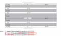
I am having 6 layer stackup for PCB and it is shown in the attached image.
L1- Signal Layer 1
L2- GND
L3- Power
L4- Signal Layer 2
L5- Vss
L6- Signal Layer 3.
Layer L1 has controlled impedance to L2 and Layer L4 has controlled impedance to L5.
I want to know that why the layer L4 is taking reference to the layer L5 why not L3 ?
Means why always signal layer chose the ground layer as reference and what will happen if it take power layer as reference ?
Thanks
Ash
Attachments
-
 24.6 KB Views: 5


