Rom memory

absf

Joined Dec 29, 2010
1,968
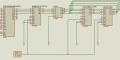
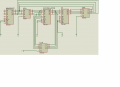
I must warn that designing a mcu is unlike building a house out of lego bricks. If you treat all the individual circuits as standard building blocks, you'd find out later that you would not be able to fit them together once your architecture and instructions set are defined.

If you want to make your job easier, you can always take a subset of the 8051 instructions and make a smaller model with less memories and 1 or 2 8-bit ports. A mcu with 2KB ROM and 256 bytes of RAM is easier to do than one with 32KB ROM and 32KB RAM.

Allen
 

Thread Starter

abhimanyu143

Joined Aug 25, 2014
211
View attachment 78024
This is the schematic for executing the above 3 instructions that I mentioned.

The truth table for the conditions of S, Y, Z, T is in the picture attached...


I have not tested it on the proteus sim. So just use it as a reference only. The S, Y, Z, T can be controlled by the outputs of the instruction decoder.

Allen
Hello Allen
as ErnieM said I have replaced mux with tristate output
upload_2015-1-2_9-0-5.png

truth table
ABCD
0010 MOV A,R
0001 MOV R,A
1110 MOV A,#5
 

Attachments

Last edited:

takao21203

Joined Apr 28, 2012
3,702
its normally not worth it to reinvent these things from zero.

You should use CPLD / FPGA its more productive. you can program the paths with software, and simulate it.

With WINCUPL you can even simulate primitive gate circuits easily.
 

absf

Joined Dec 29, 2010
1,968
Hello Allen
as ErnieM said I have replaced mux with tristate output
View attachment 78061

truth table
ABCD
0010 MOV A,R
0001 MOV R,A
1110 MOV A,#5
I have few comments about your circuit.

1. Instead of using 74240, you could use 74244 which are non-inverting buffers.
2. When doing MOV A,#5, the output from IMM DATA register would interfere with the output of REGISTER as 74HC194 outputs are not tri-state. Another tri-state buffer would be needed at the outputs of REGISTER.
3. The truth table on ABCD is not quite right. the output of 74240 is enabled with a LOW.
So it should be ..........

truth table
ABCD
0110 MOV A,R
0101 MOV R,A
0010 MOV A,#5

Allen
 
Last edited:

Thread Starter

abhimanyu143

Joined Aug 25, 2014
211
I have few comments about your circuit.

1. Instead of using 74240, you could use 74244 which are non-inverting buffers.
2. When doing MOV A,#5, the output from IMM DATA register would interfere with the output of REGISTER as 74HC194 outputs are not tri-state. Another tri-state buffer would be needed at the outputs of REGISTER.
3. The truth table on ABCD is not quite right. the output of 74240 is enabled with a LOW.
So it should be ..........

truth table
ABCD
0110 MOV A,R
0101 MOV R,A
0010 MOV A,#5

Allen
here is new circuit
upload_2015-1-3_0-31-51.png

Now I want to execute one more Instruction MOV R1#5
MOV A,R
MOV R,A
MOV A,#5
MOV R#5

I have to connect immediate register with Register R1
I don't understand how to make connection for MOV R1#5 ?
 

ErnieM

Joined Apr 24, 2011
8,377
As it is I can only guess what "MOV R#5" means since you have not defined your architecture.

Split your design work up into two parts: organization and implementation.

Organization is where you choose what functions you want to perform. How many registers, what the arithmetic/logic unit does, and a list of instructions to perform.

Implementation is where you choose what chips to use to make this happen.

You are free to loop back and fourth to adjust the organization to fit existing chips in the implementation.
 

absf

Joined Dec 29, 2010
1,968
here is new circuit
View attachment 78087

Now I want to execute one more Instruction MOV R1#5
MOV A,R
MOV R,A
MOV A,#5
MOV R#5

I have to connect immediate register with Register R1
I don't understand how to make connection for MOV R1#5 ?
Assuming your MOV R#5 means MOV R,#5 ;Load R with imm data #5

Then you could add another HC244 between ACC and R1, and connect 4 wires from o/p of U2A to inputs of R1.

Allen
 

Thread Starter

abhimanyu143

Joined Aug 25, 2014
211
Assuming your MOV R#5 means MOV R,#5 ;Load R with imm data #5

Then you could add another HC244 between ACC and R1, and connect 4 wires from o/p of U2A to inputs of R1.

Allen
I hope this is circuit
upload_2015-1-3_9-50-25.png
Now I am making circuit that will do following operation. i will post design very soon.I already have alu design .
mov accumulator #immediate data
mov accumulator , register
mov accumulator, memory
mov register , #immediate data
mov register , #accumulator
mov register , memory
mov memory #immediate data
mov memory , register
mov memory ,accumulator
 

Attachments

Thread Starter

abhimanyu143

Joined Aug 25, 2014
211
Split your design work up into two parts: organization and implementation.

Organization is where you choose what functions you want to perform. How many registers, what the arithmetic/logic unit does, and a list of instructions to perform.

Implementation is where you choose what chips to use to make this happen.

You are free to loop back and fourth to adjust the organization to fit existing chips in the implementation.
Now I have program memory , data memory , Accumulator register , 5 general purpose register, ALU, decoder ( program counter in process). I want to assemble all component to make basic processor. I know processor need another function like A/D converter , interrupt, Rs232 . I will add this function later.

I am not going to make standard processor. because I know I can't beat reputed company like Intel, IBM ..etc. I know, processor design is not easy, It need lot of experience And hard work
I don't care what I design,once I make design, than I can change or modify circuit for better performance.
that is my approach ,
 

absf

Joined Dec 29, 2010
1,968
I hope this is circuit
View attachment 78115
No, that's not correct. I said "Then you could add another HC244 between ACC and R1" and not "Add another HC244 across ACC".

You have to break the connections between ACC and R1 and insert the HC244 in between them. Try again. After completed the circuit, fill in the truth table for all the states of ABCDEF... for each instruction, like this:

ABCDEF INSTRUCTION
======================
XXXXXX MOV A,R1
XXXXXX MOV R1,A .......ETC

Now I am making circuit that will do following operation. i will post design very soon.I already have alu design .
mov accumulator #immediate data
mov accumulator , register
mov accumulator, memory
mov register , #immediate data
mov register , #accumulator
mov register , memory
mov memory #immediate data
mov memory , register
mov memory ,accumulator
It is still too soon to say this. You have to totally understand how the 4 instructions were done first before you can do those yourself. You cannot run before you know how to walk properly....:eek:

Allen
 

Thread Starter

abhimanyu143

Joined Aug 25, 2014
211
No, that's not correct. I said "Then you could add another HC244 between ACC and R1" and not "Add another HC244 across ACC".

You have to break the connections between ACC and R1 and insert the HC244 in between them. Try again. After completed the circuit, fill in the truth table for all the states of ABCDEF... for each instruction, like this:

ABCDEF INSTRUCTION
======================
XXXXXX MOV A,R1
XXXXXX MOV R1,A .......ETC


It is still too soon to say this. You have to totally understand how the 4 instructions were done first before you can do those yourself. You cannot run before you know how to walk properly....:eek:

Allen
instruction
Code:
                 A  B  C  D  E  F
mov A,#5         0  1   0  0  0  0
mov R1,#5        0  1   0  0  0  0
mov A, R1        0  0   1  0  0  0
mov R1,A         0  1   0  0  1  1
circuit upload_2015-1-4_0-8-52.png
 

absf

Joined Dec 29, 2010
1,968
instruction
Code:
                 A  B  C  D  E  F
mov A,#5         0  1   0  0  0  0
mov R1,#5        0  1   0  0  0  0
mov A, R1        0  0   1  0  0  0
mov R1,A         0  1   0  0  1  1
circuit View attachment 78153
This is the states that I got from your circuit.

Code:
                 A  B  C  D  E  F
mov A,#5         0  0   1  1  0  1
mov R1,#5        0  0   0  1  1  1
mov A, R1        0  1   1  1  0  0
mov R1,A         0  1   0  0  1  0
So can you explain how your derived the states in your answer?

There is a mistake in your circuit too. The outputs from U6A should go to outputs of U2A.

Allen
 

Thread Starter

abhimanyu143

Joined Aug 25, 2014
211
This is the states that I got from your circuit.

Code:
                 A  B  C  D  E  F
mov A,#5         0  0   1  1  0  1
mov R1,#5        0  0   0  1  1  1
mov A, R1        0  1   1  1  0  0
mov R1,A         0  1   0  0  1  0
So can you explain how your derived the states in your answer?

There is a mistake in your circuit too. The outputs from U6A should go to outputs of U2A.

Allen
I am sure , this will correct
upload_2015-1-4_7-34-7.png

truth table
Code:
A B C D E F G
0 1 0 0 0 0 0    Mov A#data
0 0 1 0 0 0 0    Mov R1#data
0 0 0 1 0 1 0    Mov A,R1
0 0 0 0 1 0 1    Mov R1,A
 

absf

Joined Dec 29, 2010
1,968
Ya, it should work. But I think U2B is not required. You can just combine the outputs of U2A, U3A & U3B together.

Allen
 

Thread Starter

abhimanyu143

Joined Aug 25, 2014
211
Ya, it should work. But I think U2B is not required. You can just combine the outputs of U2A, U3A & U3B together.

Allen
Now I want to connect data memory. so that I can execute more instruction I think I have to use 4 address line and 4 data line RAM. should I use 2114 static ram?. but there is 10 bit address bus and 4 bit data bus
 

absf

Joined Dec 29, 2010
1,968
Here's the datasheet of 2114. What can you understand from the datasheet? How are you going to implement it onto your design?

Do you know how to simulate using the proteus software?

You can use /design/new sheet on the proteus menu to add new pages under the same file name. This would prevent your design from getting oversized and hard to fit in a single piece of paper. You can link both sheets using the default/input/output labels in the "Terminal Modes" on the left of the screen. Now you should be able to have a main design called "my_mcu" and the sheets call "mov executer", "prog counter" and "alu".

Allen
 

Attachments

Last edited:
Top