Need volunteer guidance for a small PCB project (memory disability, no budget)

Thread Starter

zoinkdog

Joined Nov 16, 2025
9
Hi everyone. I’m working on a project that involves a series of small PCB boards, and I’m looking for some volunteer guidance to help me finish them.


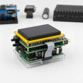
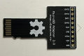
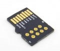
These boards are not complex; the hard part of the electronics is already done. The boards I need to make are basically connectors/adapters between two devices that already exist, kinda like a pi hat and I have drawings and clear ideas for how each board should look. I’m stuck at the stage of transferring my drawings and ideas into an actual PCB layout. I have tried my hand at easy EDA and kicad and even got as far as printing off a PCB just to find out that it didn't fit any of the parts because I had the wrong footprints and wires crossed where they shouldn't and apparently I can't have right angles on my traces .


I want to be upfront about my situation:


  • I have a memory disability, so I struggle to retain all the steps in PCB design software. I can learn parts of the workflow, but I forget things as I move forward.
  • I’m living in poverty right now, so I can’t afford to hire anyone for this.
  • I’m not asking anyone to build the boards (unless your willing) — I just need patient help translating my sketches and plans into KiCad/EasyEDA so I can finally get these small boards finished.

If someone here would be willing to volunteer a little time to walk me through the process or help me set up the first boards, I would be extremely grateful. Even small bits of help would move this project forward in a big way.


Thanks for reading, and thank you to anyone who might be able to help.
 

MrChips

Joined Oct 2, 2009
34,626
Welcome to AAC!

I don't do KiCad or EasyEDA. I can do Eagle for you.
If it is a simple board, any one with KiCad/EasyEDA experience can port a PCB layout to KiCad/EasyEDA.

Show us a schematic, BOM, and what you have attempted so far, with all relevant dimensions, hardware, component, mounting hole placements, etc.
 

panic mode

Joined Oct 10, 2011
4,864
i do KiCad... post specs and any sketch of desired layout. then you can have project and tweak it any way you like if you feel it needs final touches...
 

Thread Starter

zoinkdog

Joined Nov 16, 2025
9
The goal of this project is both educational and practical. I want to teach my son how to solder while also teaching him how to set up and use the basic functions of each module as we go, step by step.


The project will consist of a series of small, stackable PCB boards (“modules” or “hats”). The first board is the foundation and is based on the Cheap Yellow Display (CYD) — specifically the USB-C version with the extra ports.

First (Base) Board – Purpose

The first board is intended to connect to all available ports on the CYD and act as the core power and expansion board. It should include:


  • A power switch
  • A battery charger circuit
  • Pads or a footprint to solder a lithium battery
  • A boost converter (if required — I’m not yet sure whether this will be needed for future boards and would appreciate guidance here)
  • A microSD (TF) card slot
  • Additional solder pads to attach wires for a microSD breakout module that will plug directly into the CYD
Expansion and Stacking

  • The board will include a pin header layout similar to a Raspberry Pi, allowing additional boards to stack neatly on top of the first one.
  • Each future board will attach vertically, making the system modular and easy to expand as new functions are added.
  • The pinout is intended to stay consistent across boards so that stacking remains simple and intuitive.
Notes
  • Each future board should have a switch to turn the board itself on and off but just slightly offset from the prior board
  • Unfortunately, my original sketches are currently in storage, so I’m working from memory and written descriptions for now.
 

Attachments

panic mode

Joined Oct 10, 2011
4,864
stackable design has its uses but building skyscraper is going to take some room and cost more than making single PCB with places to mount everything. the slide switches could be replaced by DIP switches to make them more compact. personally i would add IO expander and mosfets so that different modules can be enabled though software or touchscreen. i'd add buzzer too. some reports on the touchscreen complain that it is not sensitive, it requires hard press. perhaps adding rotary encoder would not hurt.

1765812091450.png
 
Last edited:

Thread Starter

zoinkdog

Joined Nov 16, 2025
9
Haha, no skyscraper—just one long horizontal Lego brick to build as we learn! The stacking keeps it modular so my son learns one circuit at a time: solder, code it with Bruce (or similar flashable programming already created), test, done. Switches give us clean on-off—no ghost signals messing up the "lesson". A flat board's clever though, saves space and money, but then it's all soldered up front… kinda hard to teach that way without burying pieces under each other. Still, open to tweaks and side projects. although the one board fitting all modules would be a great end lesson to demonstrate efficiency and what a single board product would look like. and i really like your knob idea!
 

Thread Starter

zoinkdog

Joined Nov 16, 2025
9
I generated an AI image showing how I want the final assembly to look. The plan is to use the CYD as the interface, connect the first board to all 4 JST connectors, holes to solder the interface to the micro SD card on the cyd, and route call cyd connections through GPIO connectors on the 1st board. The first board will have power distribution, a micro SD card pass-through, and a power switch. I intend to create a micro SD card PCB with holes in order to solder ribbon cable to it and Sir that to the first board. Basically making it so I can plug into all ports without altering the cheap auto display for the first board
 

Attachments

Thread Starter

zoinkdog

Joined Nov 16, 2025
9
Haha, no skyscraper—just one long horizontal Lego brick to build as we learn! The stacking keeps it modular so my son learns one circuit at a time: solder, code it with Bruce (or similar flashable programming already created), test, done. Switches give us clean on-off—no ghost signals messing up the "lesson". A flat board's clever though, saves space and money, but then it's all soldered up front… kinda hard to teach that way without burying pieces under each other. Still, open to tweaks and side projects. although the one board fitting all modules would be a great end lesson to demonstrate efficiency and what a single board product would look like. and i really like your knob idea!
but i def have an all in one idea for it as well.
 
Top