Requesting Feedback on PCB Design for ESP32-C3, Sensors, and SIM808 Module

Thread Starter

achrafffff

Joined Oct 25, 2024
3
Hello everyone,

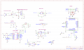
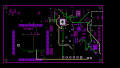
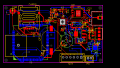
I’ve been working on a PCB design for my project, and I would appreciate any feedback or recommendations you can offer. The design includes:

  • ESP32-C3 for control and communication
  • SIM808 module for GPS and GPRS with SIM card support
  • MLX90614 for temperature measurement
  • MPU-9250 accelerometer
  • APDS-9960 proximity sensor
  • Power management using TP4056 for LiPo battery charging and switching between external power and battery
I've attached the schematic and PCB layout below. I am particularly interested in feedback on:

  1. Power supply stability, especially for the SIM808, as I’ve included components for USB/battery power switching.
  2. Any suggestions to optimize power consumption (using ESP32 deep sleep, etc.).
  3. Ensuring proper communication via I2C between the ESP32-C3 and the sensors (pull-up resistor values, etc.).
  4. Antenna placement and routing for SIM808 (GSM and GPS antennas).
Looking forward to your insights!

Thanks in advance for your help.

Schematic_esp32-v2_2024-10-24.pngPCB_PCB_esp32-v2_2024-10-25.png
 

Thread Starter

achrafffff

Joined Oct 25, 2024
3
Hello everyone,

I'm working on a 4-layer PCB design and would appreciate any feedback or recommendations you might have. Here are some key details of the design:
:heavy_check_mark:
Microcontroller: ESP32-C3FH4 for control and communication
:heavy_check_mark:
GPS/GPRS Module: SIM808, with SIM card support
:heavy_check_mark:
Sensors:
MLX90614 for temperature measurement
MPU-9250 for acceleration sensing
APDS-9960 for proximity detection
:heavy_check_mark:
Power Management: TP4056 module for LiPo battery charging and seamless switching between USB, battery, and external power
:heavy_check_mark:
Antenna Connections: Separate GSM and GPS antennas for the SIM808

:heavy_check_mark:
Layer Configuration:

:heavy_check_mark:
4-Layer Stack:
Top Layer: Signal
Inner Layer 1 : Power
Inner Layer 2 : Ground
Bottom Layer : Signal

:heavy_check_mark:
Design Goals and Specific Areas for Feedback:

1. Power Supply Stability: I'm particularly concerned about ensuring stable power to the SIM808 module. The power circuit includes components for USB/battery power switching. Any suggestions on component selection, layout, or decoupling for power stability?
2. Power Consumption Optimization: I'm exploring power-saving features such as ESP32 deep sleep. Would love advice on component adjustments or layout techniques to reduce overall consumption.
3. I2C Communication Reliability: This design involves multiple I2C devices connected to the ESP32-C3. Feedback on pull-up resistor values or tips for improving I2C communication stability would be very helpful.
4. Antenna Placement and Routing: Since I have GSM and GPS antennas for the SIM808, I want to ensure optimal placement and minimal interference. Any best practices on antenna layout, ground plane isolation, or signal routing?

I've attached the schematic and PCB layout below. Looking forward to any insights you can provide to help make this design more robust and efficient.

Thanks in advance for your help!
 

Attachments

Top