Facebook
 Google
 GitHub
 Linkedin
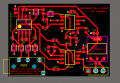
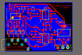
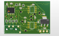
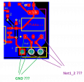
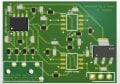
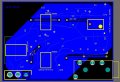
Hi! I'm a biomedical engineering student, 2nd year, very passionate about electronic. I have developed an EEG theoretically, but to make it real (pcb) i first need to practice. So i decided to make a very simple EMG (electromyography). End decided that if it will work, maybe, i will try to make a little business out of that (I have quite a lot of ideas with emgs). But first I need very solid PCB design knowledge. How does it look to you? If it is shitty, just say it XD. I haven't placed the 1 uF capacitor after the LDO nor the 10nF in parallel with the 1uF decoupling capacitors of the other ICs (called Cu1,Cu2..). I tried to make everything not compact because I will have to hand-solder it (it's 3something cm wide, so it's already pretty tiny). I also tried to not place any components on the bottom layer. Is my ground plate ok? Are the connection ok? Specifically, is the via under the "very important opamp" (an ina) ok? I think it's one of the most messy part of the pcb. I used the same trace width for simplicity: should i make the gnd and supply/reference traces bigger even if the pcb is so small? Do not hesitate if it completely sucks, I'm a very beginner and thirsty of knowledge. Thank you again!
ps: i have just noticed i accidentally let the white connection lines (ratlines). I didn't follow them as I found easier to arrange the components in different ways from the schematic.
ps: i have just noticed i accidentally let the white connection lines (ratlines). I didn't follow them as I found easier to arrange the components in different ways from the schematic.
Attachments
-
 216.5 KB Views: 56
 -
 376.6 KB Views: 57
 -
 261 KB Views: 49