Requesting advices on very first PCB design

Thread Starter

chris_051_

Joined Jul 28, 2026
6
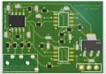
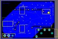
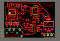
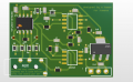
Hi! I'm a biomedical engineering student, 2nd year, very passionate about electronic. I have developed an EEG theoretically, but to make it real (pcb) i first need to practice. So i decided to make a very simple EMG (electromyography). End decided that if it will work, maybe, i will try to make a little business out of that (I have quite a lot of ideas with emgs). But first I need very solid PCB design knowledge. How does it look to you? If it is shitty, just say it XD. I haven't placed the 1 uF capacitor after the LDO nor the 10nF in parallel with the 1uF decoupling capacitors of the other ICs (called Cu1,Cu2..). I tried to make everything not compact because I will have to hand-solder it (it's 3something cm wide, so it's already pretty tiny). I also tried to not place any components on the bottom layer. Is my ground plate ok? Are the connection ok? Specifically, is the via under the "very important opamp" (an ina) ok? I think it's one of the most messy part of the pcb. I used the same trace width for simplicity: should i make the gnd and supply/reference traces bigger even if the pcb is so small? Do not hesitate if it completely sucks, I'm a very beginner and thirsty of knowledge. Thank you again!

ps: i have just noticed i accidentally let the white connection lines (ratlines). I didn't follow them as I found easier to arrange the components in different ways from the schematic.
 

Attachments

AnalogKid

Joined Aug 1, 2013
12,217
Delete the cutsie text.

Some components do not have reference designators. That will be a serious problem during debugging.

For the 5-oin connector (reference designators!), it looks like you have obround holes in the board. This will be an unnecessary cost increase.

Also, the diameter of the pads is very close to the axis length of the pin holes. A small misalignment in production will cause a breakout - the copper pad sill not be continuous all the way around the pin. You've got plenty of room to increase the diameter of the pads so there is at least 20 mils of copper all the way around. Since it is a connector, and things tug on connectors, bigger fatter pads will increase mechanical strength.

There are many places on the board where one trace joins another at an acute angle. This creates a "flux trap", and should be avoided. Adjust the traces such that they meet at 90 degrees.

I'm not a big fan of daisy-chain connections. Example, the left side of R2. If you determine that you need to disconnect R2 from that net for some reason, you have to make 2 trace cuts to isolate the pad, and add a jumper to reconnect the net around the pad. Better to run the trace near the pad and connect it with a spur. Now you can isolate the pad with a single cut and no jumper. This isn't critical (and in RF work it sometimes is avoided), but over the decades it has saved me a lot of surgery. Daisy-chaining is fast and convenient, but as a personal design rule I think it should be done only when justified.

ak
 
Last edited:

Thread Starter

chris_051_

Joined Jul 28, 2026
6
Delete the cutsie text.

Some components do not have reference designators. That will be a serious problem during debugging.

For the 5-oin connector (reference designators!), it looks like you have obround holes in the board. This will be an unnecessary cost increase.

Also, the diameter of the pads is very close to the axis length of the pin holes. A small misalignment in production will cause a breakout - the copper pad sill not be continuous all the way around the pin. You've got plenty of room to increase the diameter of the pads so there is at least 20 mils of copper all the way around. Since it is a connector, and things tug on connectors, bigger fatter pads will increase mechanical strength.

There are many places on the board where one trace joins another at an acute angle. This creates a "flux trap", and should be avoided. Adjust the traces such that they meet at 90 degrees.

I'm not a big fan of daisy-chain connections. Example, the left side of R2. If you determine that you need to disconnect R2 from that net for some reason, you have to make 2 trace cuts to isolate the pad, and add a jumper to reconnect the net around the pad. Better to run the trace near the pad and connect it with a spur. Now you can isolate the pad with a single cut and no jumper. This isn't critical (and in RF work it sometimes is avoided), but over the decades it has saved me a lot of surgery. Daisy-chaining is fast and convenient, but as a personal design rule I think it should be done only when justified.

ak
HI, thank you very much for the resposnse! The designatpors are unpractical but funny, i thought it would be cool. About the texts: why should i avoid them? do they cost a lot more?

If you mean the ''AUX'' connectr (PJ-320A), it must have the 2 holes in the center for stability (the connector has them): i chose the version with the '''through hole'' pins for stability, it should be more solid. I took the 3D model from a library, so i think it should work. I did the same with every other piece.

About the flux-trap, should't i avoid 90° connections? i thought they should be avoided.

About that R2: if you mean the one at the lower-left corner of the ''opamp'', it's a voltage divider, so that R2 has to go to ground, and i connected it to GND using a VIA.
Abut the daisy chaining: i had no idea it was i thing. Should i avoid them? when i shouwed a first prototype of my eeg pcb to my teacher, he didn't say anything about them.
Thank you very much! if you want to, i can change the names of the designators for clarity (now i called the components with same value with the same designator for semplicity)
 
Last edited by a moderator:

AnalogKid

Joined Aug 1, 2013
12,217
(now i called the components with same value with the same designator for semplicity)
no. No. NO.

My comment about daisy-chain connections is a perfect example of why you *never* do this. The R2 I used as an example and the R2 you responded about are not the same part, so the reference designation is useless. A design rule check of the schematic should have caught this, and the netlist importer of the layout software should have caught this. That raises questions about your software. AND your teacher really should have caught this, which raises other questions.

Confusion. Chaos. Heat death of the universe.

ak
 

Thread Starter

chris_051_

Joined Jul 28, 2026
6
A strong NO! All designators must be unique so that you can unambiguously name each individual part. I am surprised the software even allowed that, since it is typically how the parts in the schematic and the board are matched up.
Thank you very much! i will proceed to change their name now. Please if you have any suggestions I would be very grateful to hear them.
 

Thread Starter

chris_051_

Joined Jul 28, 2026
6
no. No. NO.

My comment about daisy-chain connections is a perfect example of why you *never* do this. The R2 I used as an example and the R2 you responded about are not the same part, so the reference designation is useless. A design rule check of the schematic should have caught this, and the netlist importer of the layout software should have caught this. That raises questions about your software. AND your teacher really should have caught this, which raises other questions.

Confusion. Chaos. Heat death of the universe.

ak
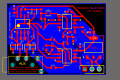
my teacher has not yet reviewed this schematic, he's on vacation probably. I have changed the designators of every components. Here's the update. How does it look?
 

Attachments

So you already know about the reference designators and making sure they are all unique and as was mentioned, they should have been that way from the schematic to the board, but I'm not an Altium user so I don't know how that tool works. You have several acute angle trace junctions like the trace that runs from C3 to R7 and the connection to pin 1 of the OP amp. Also into pads like pin 1 of the LDO component in the lower right. You should avoid acute angles like that if you can and as mentioned, a 90 deg intersection is fine. Trace widths are OK to be the same for signals and if you want to increase them for the power and ground lines, you can but on a small board like this, might not be a big issue, but if you have any high speed signals, its better to have a wider trace for power and ground. It's good practice to not have a trace connect 2 pins that are next to each other directly and its better to pull out a small "U" between the pins. Like OP Amp 2 right side 2nd and 3rd pins. This can look like a short to assemblers or even a fabrication shop and they might try to remove it when its really supposed to be connected. Pull those traces out to make that "U" shape to also allow you to cut the trace easier if you needed to. You should also extend that ground plane, (blue area in second picture) out to under the red trace running diagonally to give you a good return path which might help reduce noise if your signals are low level, etc. For a first time out, it doesn't look too bad. ;-) Good luck on your project...
 
How does it look to you? If it is shitty, just say it XD.
well.. you asked for it... ;)


first of all where is the schematics? are you sure you got things right?

EEG is sensing very small signals (sensitive to noise) so parts selection and layout are important. you were already told that if you are serious about getting professional opinion, you may want to get serious yourself and strip all the juvenile texts (it is off-putting), and use unique and standardized reference designators etc. for example reference ICs U1, U2, U3 etc. not Amplifier, Amplifier1, Something and similar.
once you get the feedback you want, you can always go back and cover it with graffiti all you like.

second of all, this will not work.

you want to keep the noise level down. this means picking low noise parts. ADS1117 is "ok" but not great part here. also it has massive quiescent current of 10mA. that is more than current draw of the rest of the circuit. and large currents are generally greater source of EMI. it is hard to have accurate recording of a whisper next to a thunderous waterfall.
situation can be improved (to a degree) with careful layout and capacitors. but - they are missing. you only have a single cap before and after regulator. you may want to check EEVblog vide on bypass caps - both around regulator and around each of the ICs. this exact regulator stability depends on capacitors it can oscillate (too low ESR is not good).

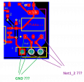
but that is not even it - i am pretty sure you also have it miswired. not surprising, since you were more concerned with verbal nonsense instead of labeling board connections. if you did the right thing, you would have probably see it yourself.

1785600798983.png

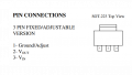
Proper pinout is found in the datasheet:
1785601184867.png
so if you are keeping it, you may want to carefully chose capacitors around it. so do NOT put large value MLCCs around it - their ESR is close to zero. i would put 0.1uF ceramic before and after it (which is probably what you have already), then add 22uF tanalum or alu electrolytic (not ceramic!!!) after it. and then at LC filter to sensitive analog stage (ferrite beas or small inductor such as 4.7uH) and another 10uF cap. still highly recommended options for medical grade AFE would be ICs with better specs like LT3042.
 

Thread Starter

chris_051_

Joined Jul 28, 2026
6
well.. you asked for it... ;)


first of all where is the schematics? are you sure you got things right?

EEG is sensing very small signals (sensitive to noise) so parts selection and layout are important. you were already told that if you are serious about getting professional opinion, you may want to get serious yourself and strip all the juvenile texts (it is off-putting), and use unique and standardized reference designators etc. for example reference ICs U1, U2, U3 etc. not Amplifier, Amplifier1, Something and similar.
once you get the feedback you want, you can always go back and cover it with graffiti all you like.

second of all, this will not work.

you want to keep the noise level down. this means picking low noise parts. ADS1117 is "ok" but not great part here. also it has massive quiescent current of 10mA. that is more than current draw of the rest of the circuit. and large currents are generally greater source of EMI. it is hard to have accurate recording of a whisper next to a thunderous waterfall.
situation can be improved (to a degree) with careful layout and capacitors. but - they are missing. you only have a single cap before and after regulator. you may want to check EEVblog vide on bypass caps - both around regulator and around each of the ICs. this exact regulator stability depends on capacitors it can oscillate (too low ESR is not good).

but that is not even it - i am pretty sure you also have it miswired. not surprising, since you were more concerned with verbal nonsense instead of labeling board connections. if you did the right thing, you would have probably see it yourself.

View attachment 370037

Proper pinout is found in the datasheet:
View attachment 370038
so if you are keeping it, you may want to carefully chose capacitors around it. so do NOT put large value MLCCs around it - their ESR is close to zero. i would put 0.1uF ceramic before and after it (which is probably what you have already), then add 22uF tanalum or alu electrolytic (not ceramic!!!) after it. and then at LC filter to sensitive analog stage (ferrite beas or small inductor such as 4.7uH) and another 10uF cap. still highly recommended options for medical grade AFE would be ICs with better specs like LT3042.
thank you very much! First of all, very much sorry, I didn't specify it: this is an EMG. opsie, the EEG is quite more complex (I have it, if you want to i can upload the schenatics too).
I didn't think about LC filters at all! I will add them surely.
As i said, i didn't followed the schematics properly and i switched some parts. I have already corrected them today as my teacher also suggested me to do so. This project is definitely not meant to be a medical grade one, but I will try to follow some guidelines. I will definitely adjust the decoupling capacitors, including the LDO ones (i used a 4,7uF parallel to a 100nF, both X5R 0603 format. I will change the 4,7uF with a tantalum one :))
Initially i designed an EEG with 8 electrodes, very precise components and costly opamps (fortunately I got the saples, valued at 52€ if i remember correctly). But i realize I need some solid experience first (with soldering too!). And I will adjust that pcb with all the precious advices this community gave me, too. So i developed this one with cheaper pieces: the instrumental opaamp is from analog devices (AD8262 if i remember correctly); the opamps are the AS2333 from diodes incorporated, with crazy specs for their prices (they are explicitly intended for wearable medical devices, so they should work out), the LDO..well, already commented, i might change that in the following days; I have added a pnp mosfet (AP3407A) for battery polarity protection. All resistors are 1% and i changed the format from 0603 to 0805 for easier soldering, while some capacitors are C0P (smaller capacitance ones), while most are, unfortunately, X7R (couldn't find cheap 100nf C0P or couldn't find them at all), 0603 format for stability. Unfortunately they will definitely add some noise and i very much it hope it won't be as disasterous as I think based on my little knowledge about capacitor types. My teacher suggested me to extend the ground plate to both layers and fill everything with it as much as possible, so I will do so. He also suggested me to avoid 90° routes and avoid vias where routes encounter (something i did frequently). The ground plate on the upper layer should also help with decoupling capacitors and everything that is connected to ground (so i will need way less vias).
I will upload an updated version of it if you want to!
Thanks again ;)
 
I dont know anything about your circuit or its functions so wont get into that but for the over all look of it:

The text and missing designators on silkscreen I dont mind at all. I tend to leave those off my boards all the time, You have the schematics so its not a big deal imo.
.
The layout and trace routing is pretty bad though.

Is there a functional reason why the fill zone is not the entire top and bottom layers?
 
Top