Request for help in repairing Technics SU-V90D

Thread Starter

KaMel88

Joined May 11, 2026
48
One is not better than the other. One can dissipate more power than the other.
One, you need to purchase 2000 pieces. The other, you can buy as many as you need.
I understand that it will be good no matter which one I choose. My main concern is whether the resistor type is good. Or do you recommend something else?
 
Last edited:

MrChips

Joined Oct 2, 2009
35,044
Z551/Z552 are 0.22 Ω emitter power resistors. The resistor provides a number of functions.

  1. Limits the current through the power transistor
  2. Raises the voltage on the emitter of the transistor, reducing the base-emitter bias voltage
  3. Shifts the operation mode from Class-B towards Class-AB, reducing cross-over distortion
  4. Provides negative feedback and temperature stability, improving linearity

3 W power rating is underrated. 5 W power is an improvement.

5 W power dissipation will occur with 5 A through a 0.2 Ω resistor, using the formula,
P = I x I x R

5 A into an 8 Ω speaker is 200 W.

In other words, the resistor has to dissipate 5 W when driving an 8 Ω speaker at 200 W.

Edit:
3.5 A into an 8 Ω speaker is 100 W
3.5 A into a 0.22 Ω resistor 2.7 W.
3 W resistor will work, 5 W gives extra headroom.
 

Thread Starter

KaMel88

Joined May 11, 2026
48
We don't yet know which components caused the catastrophic failure. Our focus is on getting the LEFT channel working so that we can get some real live voltages. I am contemplating replacing Q551 in the LEFT channel as a first stab at it.
Q551 replaced with a new one, voltages unchanged:
E: -6
C: -3,7
B: -5,3
 
Last edited:

MrChips

Joined Oct 2, 2009
35,044
For reference only, I am looking at the circuit for the LEFT channel. (Of course, the RIGHT channel will be identical.)
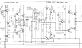
I cannot get the simulator to arrive at the same voltages as shown in the service manual below.

1788053157434.png

I don't understand what IC501, Q501, Q503, Q505, Q507 do.

Output stage Q553, Q555, Q557, Q559 is a classic configuration. Q551 is the driver stage but I don't see how it gets biased properly.

There is feedback from (a) via R573 (1-ohm) to zener diodes D501 and D503. On the simulator, this feedback is going to drive the Q501 and Q503 outputs which are the supply voltages of IC501. Thus, IC501 supply voltages change with signal content.

I am inclined to ignore IC501, at least for a test.
What are the voltages at TP401 (1) (2) and (3) ?
 

Thread Starter

KaMel88

Joined May 11, 2026
48
For reference only, I am looking at the circuit for the LEFT channel. (Of course, the RIGHT channel will be identical.)
I cannot get the simulator to arrive at the same voltages as shown in the service manual below.

View attachment 370856

I don't understand what IC501, Q501, Q503, Q505, Q507 do.

Output stage Q553, Q555, Q557, Q559 is a classic configuration. Q551 is the driver stage but I don't see how it gets biased properly.

There is feedback from (a) via R573 (1-ohm) to zener diodes D501 and D503. On the simulator, this feedback is going to drive the Q501 and Q503 outputs which are the supply voltages of IC501. Thus, IC501 supply voltages change with signal content.

I am inclined to ignore IC501, at least for a test.
What are the voltages at TP401 (1) (2) and (3) ?
I measured the voltages for TP401 and TP402. The measurement at both points is the same.
1: -0,1
2: 0
3: 0,1
 

MrChips

Joined Oct 2, 2009
35,044
I measured the voltages for TP401 and TP402. The measurement at both points is the same.
1: -0,1
2: 0
3: 0,1
Ok. Thanks for the readings. This is a good sign and what I would expect.

Before moving on, I should point out that when it comes to repairing something very complex as this, it helps to get a good understanding of how the circuit works. Technics has done a fair job of labeling the function of the different sections of the circuit.

You will notice that the section labelled VOLTAGE CONTROL AMP with Q413-Q419 is similar to the POWER AMP Q553-Q559.

The VOLTAGE CONTROL AMP itself looks like the output stage of a power amp. The difference here is that it is designed to provide voltage gain but with little power output.

The POWER AMP Q551-Q559 has voltage gain of 1 but provides high current output to a low impedance load.
 

Thread Starter

KaMel88

Joined May 11, 2026
48
We need to find what controls the bias voltages on Q551.

Remove IC501 and tell me again what components are removed from the board.
I desoldered IC 501.
Pin voltages after desoldering:
1 : 0v
2 : 0v
3 : 7,89v
4 : -7,85v
5 : 0v
6 : 0v
7 : 7,89v
8 : 7,89v

Currently desoldered components:
R560
R558
Q556
Q554
Q504
Q502
Q552
Z552
IC502
IC 501

Q560/Q559
Q558/Q557
 

MrChips

Joined Oct 2, 2009
35,044
Basically, all the parts removed are on the RIGHT channel.
I had suggested that you install 8-pin DIP sockets for IC501 and IC502. This would allow for easy removal and insertion of the ICs.

At IC501, pin-3 and pin-7 are direcly connected to the base of Q551. The voltage of 7,89 V does not match a previous measurement of Q551 on post #86.
Q551 replaced with a new one, voltages unchanged:
E: -6
C: -3,7
B: -5,3
Can you check the voltages on Q551 again?
 

Thread Starter

KaMel88

Joined May 11, 2026
48
Basically, all the parts removed are on the RIGHT channel.
I had suggested that you install 8-pin DIP sockets for IC501 and IC502. This would allow for easy removal and insertion of the ICs.

At IC501, pin-3 and pin-7 are direcly connected to the base of Q551. The voltage of 7,89 V does not match a previous measurement of Q551 on post #86.


Can you check the voltages on Q551 again?
I have already installed DIP sockets in both channels.
You are right, now the current on q551 looks different :
Q551 - on all legs B,C,E = 7,88v
 
Top