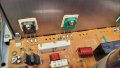
You are doing something wrong. As far as I can see, the curved side is against the pressure clip for both transistors.
The flat side faces the main heat sink.
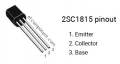
Before replacement, TS checked pinout in datasheet and see discrepancy between pinout and silkscreen.
So, questions:
1. What, in reality, was original orientation?
2. This metal thing is "heatsink" or it is some mechanical part? Some clip?
Before replacement, TS checked pinout in datasheet and see discrepancy between pinout and silkscreen.
So, questions:
1. What, in reality, was original orientation?
2. It metal thing is "heatsink" or it is some mechanical part?
I don't know what discrepancy TS found. I see no discrepancy with datasheet, PCB holes and silkscreen.
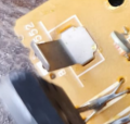
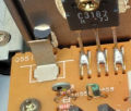
The metal thingy is a pressure clip to push the transistor's flat face against the metal back plate "the heatsink".
You can see in the photo, heatsink compound between the flat face of Q551 and the "heatsink".
original Japanese transistors used in locations like Q551 require the flat side to face backward toward the thermal clip and heatsink while maintaining the E-C-B pinout from left to right.
The metal thingy is a pressure clip to push the transistor's flat face against the metal back plate "the heatsink".
You can see in the photo, heatsink compound between the flat face of Q551 and the "heatsink".
Sorry for the confusion. I didn't read that it was a bottom-up view. Later, I was stuck with my mistake. Please remove the unnecessary posts from the thread as I've caused a bit of confusion.
I made a very stupid mistake...
One possible source for confusion is that the Technics Service Manual for SU-V90D shows the circuit board as viewed from the solder side. Yet, they reversed the component reference designators so that you can identify the component. This is not the silk screening that one would find on the component side of the PCB.
Here is the image of the PCB as viewed from the component side.
Not yet. The voltages look reasonable, except Q559 base should be -0,5 V.
I suppose the readings were taken with the lamp circuit.
What are the readings if you remove the lamp circuit?
Not yet. The voltages look reasonable, except Q559 base should be -0,5 V.
I suppose the readings were taken with the lamp circuit.
What are the readings if you remove the lamp circuit?
When you can get 0 V at the emitters of both Q557 and Q559 you can do an audio test.
Turn the VOLUME control down to the lowest level. Connect a loudspeaker to the LEFT channel output.
Apply audio source and turn up the VOLUME control slowly. Do not test at high sound level.
Listen to the quality of the sound and listen for noise or distortion, or if you get any sound at all.
When you can get 0 V at the emitters of both Q557 and Q559 you can do an audio test.
Turn the VOLUME control down to the lowest level. Connect a loudspeaker to the LEFT channel output.
Apply audio source and turn up the VOLUME control slowly. Do not test at high sound level.
Listen to the quality of the sound and listen for noise or distortion, or if you get any sound at all.
Not necessary if you keep the test short and at low volume. Check the temperature of the transistors with your finger as soon as you turn the power on. Turn off immediately if the transistors are too hot to touch. (I use a thermal imaging camera when I do these tests.)
To be on the safe side, you can add individual cooling fins to Q557 and Q559. Do not allow the metal fins to touch each other or any part of the amplifier and chassis. Keep the fins isolated from everything else.
Not necessary if you keep the test short and at low volume. Check the temperature of the transistors with your finger as soon as you turn the power on. Turn off immediately if the transistors are too hot to touch. (I use a thermal imaging camera when I do these tests.)
To be on the safe side, you can add individual cooling fins to Q557 and Q559. Do not allow the metal fins to touch each other or any part of the amplifier and chassis. Keep the fins isolated from everything else.
When you can get 0 V at the emitters of both Q557 and Q559 you can do an audio test.
Turn the VOLUME control down to the lowest level. Connect a loudspeaker to the LEFT channel output.
Apply audio source and turn up the VOLUME control slowly. Do not test at high sound level.
Listen to the quality of the sound and listen for noise or distortion, or if you get any sound at all.
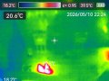
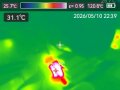
The left channel works. Music sounds good, without distortion, and I listened for about 15 minutes. I also used a thermal imaging camera. The transistors remained cool throughout the test, with only the bridge rectifier area exceeding 100°C.
That is good news. Now you have a working LEFT channel by which you can compare voltages with the bad RIGHT channel.
Use the lamp circuit at this stage to limit the current.
Start by measuring the voltages at TP402 to make sure that they are close to 0 V.
Install the missing components and check the voltages at the transistors.
Measure the resistors before installing. Do a diode test on the transistors before installing.
Key voltages we are looking for are:
Q558, Q560 emitters, Z552 should be 0 V.
IC502 pin-8, 7 to 8 V
IC502 pin-4, -7 to -8 V
Q554 base, about 1 V
Q556 base, about -1 V
That is good news. Now you have a working LEFT channel by which you can compare voltages with the bad RIGHT channel.
Use the lamp circuit at this stage to limit the current.
Start by measuring the voltages at TP402 to make sure that they are close to 0 V.
Install the missing components and check the voltages at the transistors.
Measure the resistors before installing. Do a diode test on the transistors before installing.
Key voltages we are looking for are:
Q558, Q560 emitters, Z552 should be 0 V.
IC502 pin-8, 7 to 8 V
IC502 pin-4, -7 to -8 V
Q554 base, about 1 V
Q556 base, about -1 V
1. Normally, it is best to do it in stages. However in this case, there is DC feedback involved in this circuit. So we have to take the chance and hope that all the components are good.


 Facebook
 Google
 GitHub
 Linkedin