Im wondering how much i can learn from the labelling of the pinouts of the CD4060 in terms of conventions in the IC industry.
For example, output pins 9, 10 and 11 form the oscillator stage of the CD4060 IC. They appear to be labelled using the symbol for theta. How are they referred to in speech? My guess is listed below. Is the following list anywhere near the mark?
11 = “theta 1”
10 = “theta 0 hat”
9 =”theta 0”
What is the significance of the subscripts?
Why is this greek letter used and not another letter from the greek alphabet?
On every datasheet I've seen, those pins are P0, -P0 (shown as P0 with an overhead bar), and P1. Theta is the symbol for phase, which is one reason why it was changed to P. The other is that typesetters (think 1960's) and anyone with a keyboard hate special characters.
Flipflop outputs have been referred to a Q this and that forever. Don't know why.
On every datasheet I've seen, those pins are P0, -P0 (shown as P0 with an overhead bar), and P1. Theta is the symbol for phase, which is one reason why it was changed to P. ak
The Fairchild DS you sent me uses these theta symbols
The theta symbols also appear in each of the flip flop modules in the the one called "fairchild logic diag".
My question is nonetheless - whether they are theta or P- what is P (or theta) symbolic of? what sets these apart?. and is there are rationale for them using P or theta for this class of pinouts?
The Greek letters θ, theta, and Φ, phi, are commonly used in geometry as symbols for angles.
In electronics, they are used to represent phase angle.
In this context, P and P' are used to indicate that these are two signals that are 180° out of phase. These two signals originate from the inverter oscillator circuit that is meant to be driven from an external quartz crystal.
btw, the symbol in the data sheet is phi, Φ (pronounced fy as in fly), not theta.
The Greek letters θ, theta, and phi, Φ, are commonly used in geometry as symbols for angles.
These two signals originate from the inverter oscillator circuit that is meant to be driven from an external quartz crystal.
.
The Greek letters θ, theta, and phi, Φ, are commonly used in geometry as symbols for angles.
In electronics, they are used to represents phase angle.
In this context, P and P' are used to indicate that these are two signals that are 180° out of phase. These two signals originate from the inverter oscillator circuit that is meant to be driven from an external quartz crystal.
btw, the symbol in the data sheet is phi, Φ (pronounced fy as in fly), not theta.
i am afraid i am out of my depth.
I looked at this article on phase difference and it implies there are two wave forms from the oscillator separated by time. you would expect this since that is its job to keep generating a wavelength(s) in a given time period. https://en.wikipedia.org/wiki/Phase_(waves)#Phase_difference
Yes. And, I'm stupid. I've been using P0 and P1 for this part for decades, and completely forgot about the Phi marking.
P1, P0-, and P0 are the inputs and outputs of two inverters in series, so the states of those pins always are 1-0-1 or 0-1-0. We'll call the inverters Left and Right.
Start at the moment P0 goes high.
The voltage across a capacitor cannot change instantaneously, so this pulls the timing node (Rx-Cx-Rs) high. This puts a high at P1 (the Left input). It tries to put a high at P0- through Rx, but P0- is held low by the Left output.
This operating state is stable, because two inverters in series forms a latch due to positive feecback: P0 is high, P1 is high, P0- is low, P0 is high.
But while this state is stable, there is a voltage across Rx because the left end of Cx is high but P0- is low. So Cx discharges through Rx into the P0- low output of the Left inverter.
After a time, the voltage at the Rx-Cx-Rx node is low enough that Left input P1 sees it as a logical low, and Left changes state.
P1 is low, P0- goes high, P0 goes low.
Now everything is reversed from where we started, and Cx starts charging in the opposite direction.
Describing an oscillator in text always is difficult, so try to digest this and ask away.
While I am trying to figure out yesterday's posts (#142 to #149), about the phase shifting of the oscillator, I wanted to ask you about something else.
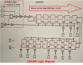
This question is about the the open circle symbol in many of the circuits I have come across so far to do with ICs like the CD4060 and the CD4017 as well as logic gate circuits in general.
I have picked out four examples listed below. On the image in each one I have circled in red the symbol I am referring to. The little open circle appears at the junction of some circuit connections and not others. In Figure 2 I have also highlighted those logic symbols which do not have the small open circle. I have used a blue dotted circle for these cases.
I am asking this question about basic circuitry symbols, as I have done before, to see if I can learn specific things from this particular IC project that I can generalise about in the future as I come across different circuits and different ICs.
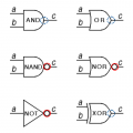
The circle indicates an active low.
For example, in the NOT gate, the input does not have the circle so it shows the input is "active" when it is High. BUT the output will be Low. So for a NOT gate, the output is NOT what the input is, that is, the reverse. So it is commonly called an Inverter.
In this circuit of a 74ACT139 dual 1 of 4 decoder below, you can see it.
The Y outputs go LOW one at a time when active.
And the G inputs turn the decoder on when they are Low.
You may notice the G inputs have a line above them and this too is a way of writing that the active state is low.
I hope that helps a bit.
While I am trying to figure out yesterday's posts (#142 to #149), about the phase shifting of the oscillator, I wanted to ask you about something else.
This question is about the the open circle symbol in many of the circuits I have come across so far to do with ICs like the CD4060 and the CD4017 as well as logic gate circuits in general.
The open circle symbol is, in this context, usually referred to as a "bubble" and is used to indicate that a logic input needs to be driven low to be asserted, and a logic output will be true when it goes low. Either condition is referred to as being "low true".
For example, in the case of an SN74HC74, where the SET and RESET inputs are bubbled, in order to drive Q low and Qbar high simultaneously, RESET must be driven low while SET is high, and to drive Qbar high and Q low simultaneously requires that SET be driven low while RESET is high.
Another term used to describe this is "active high" or "active low". For example, the 4017 Enable input has a bubble, and the EN name has a bar over it. Both of these mean the same thing, that the counting function is ENabled when that input pin is low. A text description would be an active low enable.
As you roam the innergoogle you probably will come across things written by true logic purists. These people do not like it when a signal between parts has a bubble on one end but not the other. For example, if you put an inverter after a NAND gate, the resulting signal is an AND function. But that inverter has a bubble on its output, indicating that it is active low, while the AND function is defined as active high. panic ensues. The solution is to draw the inverter with a bubble on its input but not on its output. The inverting function still is clearly indicated, but now the bubble output of the NAND drives a bubble input of the inverter, and the inverter output has no bubble, consistent with the overall AND function.
Fun, huh?
Actually, this is not just pedantic purist bubble babble. CPLD and FPGA are two types of large-scale, complex logic devices with hundreds of thousands of internal gates, and the internal gates can have dozens of inputs. To keep logic polarities and active states straight, it is common to have gates with both bubble (inverting) and straight line (non-inverting) inputs.
The circle indicates an active low.
For example, in the NOT gate, the input does not have the circle so it shows the input is "active" when it is High. BUT the output will be Low. So for a NOT gate, the output is NOT what the input is, that is, the reverse. So it is commonly called an Inverter.
In this circuit of a 74ACT139 dual 1 of 4 decoder below, you can see it. View attachment 126486
The Y outputs go LOW one at a time when active.
And the G inputs turn the decoder on when they are Low.
You may notice the G inputs have a line above them and this too is a way of writing that the active state is low.
I hope that helps a bit.
The open circle symbol is, in this context, usually referred to as a "bubble" and is used to indicate that a logic input needs to be driven low to be asserted, and a logic output will be true when it goes low. Either condition is referred to as being "low true".
For example, in the case of an SN74HC74, where the SET and RESET inputs are bubbled, in order to drive Q low and Qbar high simultaneously, RESET must be driven low while SET is high, and to drive Qbar high and Q low simultaneously requires that SET be driven low while RESET is high.
Another term used to describe this is "active high" or "active low". For example, the 4017 Enable input has a bubble, and the EN name has a bar over it. Both of these mean the same thing, that the counting function is ENabled when that input pin is low. A text description would be an active low enable.
As you roam the innergoogle you probably will come across things written by true logic purists. These people do not like it when a signal between parts has a bubble on one end but not the other. For example, if you put an inverter after a NAND gate, the resulting signal is an AND function. But that inverter has a bubble on its output, indicating that it is active low, while the AND function is defined as active high. panic ensues. The solution is to draw the inverter with a bubble on its input but not on its output. The inverting function still is clearly indicated, but now the bubble output of the NAND drives a bubble input of the inverter, and the inverter output has no bubble, consistent with the overall AND function.
Fun, huh?
Actually, this is not just pedantic purist bubble babble. CPLD and FPGA are two types of large-scale, complex logic devices with hundreds of thousands of internal gates, and the internal gates can have dozens of inputs. To keep logic polarities and active states straight, it is common to have gates with both bubble (inverting) and straight line (non-inverting) inputs.
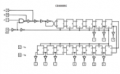
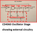
The logic diagram of the CD4060 in Figure 1, below, shows the two functional sections of the IC: the oscillator stage and the digital counter stage.
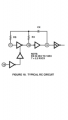
Focussing on the oscillator section, Figure 2 reproduces from Figure 1 the oscillator’s logical components and also shows the external circuitry which completes the functioning oscillator stage. It appears that two rectifiers are connected in series across Pins 11, 10 and 9. I think these rectifiers are actually a type or types of transistors.
I want to learn more about how the oscillator section of the CD4060 works by making another circuit from scratch that would replicate the workings of the internal oscillator – but not using any IC components.
Is it possible to build such as circuit without using ICs, ie transistors etc?
Due to the timing of technologies, I learned about TTL before I saw a DEC flip chip. As soon as I saw one I thought about an all discrete digital clock, followed quickly by another thought - no idiot would ever ...
Focussing on the oscillator section, Figure 2 reproduces from Figure 1 the oscillator’s logical components and also shows the external circuitry which completes the functioning oscillator stage. It appears that two rectifiers are connected in series across Pins 11, 10 and 9. I think these rectifiers are actually a type or types of transistors.
I want to learn more about how the oscillator section of the CD4060 works by making another circuit from scratch that would replicate the workings of the internal oscillator – but not using any IC components.
Is it possible to build such as circuit without using ICs, ie transistors etc?
Those are not rectifiers. Those are inverters. Everything about this type of oscillator involves ones, zeros, and transition levels.
For standard 5 V TTL logic and all other types that are compatible, a logical 0 is any voltage below 0.8 V and a logic 1 is any voltage above 2.4 V. That gap between the two is called the noise margin, and signals in that band are forbidden. Separate from those rules is the way a logic device input actually functions. For normal TTL and CMOS parts the input stage recognizes only one voltage; anything below it is a zero, and anything above it is a one. A simple logic gate actually is a very high gain linear amplifier acting as a comparator. In fact, you can use some CMOS gates as audio amplifiers. But I digress...
For TTL and many other circuits, the actual transition voltage is around 1.8 V. When the output at pin 9 changes state, so do the input at pin 11 and the output at pin 10. As explained above, this puts a voltage across R1 and the resulting current charges Cx. The junction of R1 and Cx is the input voltage to pin 11, and this is what changes slowly. Eventually (depending on the R1-Cx time constant), the input at pin 11 crosses that input's transition level, and everything flips over to the other half-cycle of the oscillator.
It is entirely possible to build this kind of oscillator with discrete transistors, but I think that is unnecessary effort. To learn more with less work, consider building it using sections of a hex inverter or quad NAND gate. Since you don't need a reset pin and are not driving other loads, you need only two inverters to reproduce this oscillator.
Important - Above I mentioned "normal" TTL and CMOS parts. Surprise, the gates in this circuit are not normal. When the input voltage changes very slowly, there can be a time as it creeps across the transition level that the output is neither a 1 nor 0, but a noise burst. This is because a gate really is a linear amplifier at heart. The solution is called hysteresis, and this explanation could get very detailed and confusing. You can read all about it, but those details are not critical to experimenting with this circuit. Suffice to say that you should use gates with hysteresis, such as the CD4093 or CD40106.
 Facebook
 Google
 GitHub
 Linkedin