Facebook
 Google
 GitHub
 Linkedin
This is a continuation of a thread here about troubleshooting PN4392 transistors. That either wasn't the issue or it got resolved, there's still something else going on.
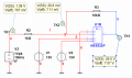
I have designed and built an acoustic guitar preamp. It has a bunch of EQ and gain sections, focused on acoustic guitar.
(Previous thread of a previous version).
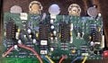
The current PCB's are 4 layer I designed in EasyEDA, outer 2 signal, inner ground and power. +/- 15v on Vcc/Vee.
I can input a tone at the input A from a signal generator and it gets stuck at pin6 of IC1... but the tone's there at pin 7. That's weird, and it's not just going through the 50k pot, if I remove IC1 it's much less - if it's going through IC1.2, then why can't I read it at pin 6? Same thing with IC2, the tone is there at IC2 pin 1, but not at pin 2.
I probed around and noticed the impedance between Vcc/Vee to a lot of components is only 670 kΩ... to me that seems low.
I'm not sure what else to check. I've got a good scope, I'm sure there are tools there that could help me beyond what I'm doing if I knew what to do.


View attachment IMG_7904.jpeg
I have designed and built an acoustic guitar preamp. It has a bunch of EQ and gain sections, focused on acoustic guitar.
(Previous thread of a previous version).
The current PCB's are 4 layer I designed in EasyEDA, outer 2 signal, inner ground and power. +/- 15v on Vcc/Vee.
I can input a tone at the input A from a signal generator and it gets stuck at pin6 of IC1... but the tone's there at pin 7. That's weird, and it's not just going through the 50k pot, if I remove IC1 it's much less - if it's going through IC1.2, then why can't I read it at pin 6? Same thing with IC2, the tone is there at IC2 pin 1, but not at pin 2.
I probed around and noticed the impedance between Vcc/Vee to a lot of components is only 670 kΩ... to me that seems low.
I'm not sure what else to check. I've got a good scope, I'm sure there are tools there that could help me beyond what I'm doing if I knew what to do.
View attachment IMG_7904.jpeg