Problems snubbing HF noise on flyback transistor

Thread Starter

Jdo300

Joined Oct 14, 2007
9
Hello,

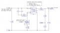
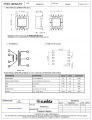
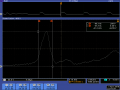
I am working on the design of a flyback converter based on the LT3751 capacitor charging circuit. My design is similar to the 42 A cap charger example on pg. 25 of the LT3751 datasheet. In my case, the circuit runs on 12V and steps up the output to 430 V, but I am having some major noise issues with the MOSFET driving the primary of the transformer. The flyback powers some other high voltage circuitry and the noise from the FET during turn-off is radiating into the other parts of the design, both through the power and ground lines and through the air.

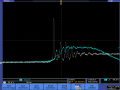
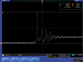
My first attack plan was to add an RC/RCD snubber across the primary of the transformer to snub the high frequency oscillations on the switch. But for some reason, none of the values I calculated for it, (or just plan experimented with) had any real impact on the waveform -- in particular, the first high voltage spike, which is rising to as high as 200V. I have attached scope shots of the turn-off waveform, including a closeup of the first spike, which is around 12 ns wide. One challenge is that this waveform's spike is so narrow, and also the waveform seems to be rich in harmonics.

Has anyone run into problems like this before or seen a waveform such as this which seems to defy normal RC/RCD snubbers? I'm not sure what to try next to remove this noise.

- Jason O
 

Attachments

Marc Sugrue

Joined Jan 19, 2018
222
Hi, Adding a snubber is only going to Clip/Disipate the energy of the oscillation it won't eliminate it so you may need to look closer at the root cause of the leakage spike in my opinion. You could look at introducing a low leakage, screened transformer and i'm assuming you made a careful layout of the printed circuit board in regards to EMI (GND planes etc). My only other suggestion based on the data you've supplied would be take a look at the primary transformer current (ideally using a current probe) and make sure the current waveforms are textbook for a flyback in the mode its designed to operate.
 

MisterBill2

Joined Jan 23, 2018
27,366
Every part of designing flyback power supplies is complex and also tricky. In many cases a voltage spike is caused by a too-fast di/dt, which in turn is caused by some portion of the circuit impedance having a frequency response that was not intended and is thus not slowing things down as it should. This sort of problem can include unintended impedances in connections, since at higher currents it does not take much impedance to develop some voltage.
The complexity is why I purchase power supplies from reputable and skilled manufacturers instead of fighting with design efforts.
 

ebp

Joined Feb 8, 2018
2,332
The initial spike is due to leakage inductance which cannot be completely eliminated no matter how the transformer is built. The leakage inductance can be minimized by careful design of the winding, for example by splitting the secondary and winding half underneath and half over top of the primary (usually done the other way, when Vout is less than Vin).

To properly measure the spike it is necessary to use a probe tip grounder, preferably with a probe with very low capacitance.

The input supply must have a good high-frequency capacitor located so as to minimize the area of the loop involving the transformer, FET, and sense resistor.

Snubber components must perform well at high frequency, which means minimal lead lengths and ceramic capacitors. Diodes are normally ultrafast recovery, though with care a slow diode can be used to shift some of the snubber capacitor discharge to the FET.

The rectifier on the secondary must have fast forward recovery and there must be a good high frequency capacitor, again with minimal loop area, on the secondary. Inductance in the connections to the secondary components reflects to the primary as additional leakage inductance.

Sometimes a judiciously placed lossy ferrite bead, typically in the FET drain circuit, can help with the highest frequency components.

Without photos and a schematic, it is all guesswork as to what might help.
 

Thread Starter

Jdo300

Joined Oct 14, 2007
9
Hello Everyone,

Thank you all for the insightful responses. I have attached some additional information about the circuit for you to check out. It is clear that there are multiple things going on with this design, and I'm beginning to wonder if I may need to re-layout the board to minimize the primary and secondary current loops. Anyway, here's the schematic, as well as the datasheet for the transformer I"m using. Since It was a customized, off-the-shelf device, I'm not sure how it was wound internally. I will find out from the manufacturer and get back with you here.
 

Attachments

Thread Starter

Jdo300

Joined Oct 14, 2007
9
To properly measure the spike it is necessary to use a probe tip grounder, preferably with a probe with very low capacitance.
What exactly is a "probe tip grounder"? Are you referring to the standard, clip-on alligator ground clip on the scope probe or some other, separate attachment?

The rectifier on the secondary must have fast forward recovery and there must be a good high frequency capacitor, again with minimal loop area, on the secondary. Inductance in the connections to the secondary components reflects to the primary as additional leakage inductance.
Thank you again for this insight here. Referring to the high frequency capacitor on the secondary side, are you saying that it should be connected directly across the secondary winding itself, or should it go in parallel with the larger output capacitance on the DC side of the output?
 

Marc Sugrue

Joined Jan 19, 2018
222
Looking at the circuit there's a number of things i believe you should provision for.

C11 should be a high quality capacitor such as a Film Cap. Located Right next to pins 1& 2 of the Transformer.
The Bottom of the Capacitor should go through to a solid 0v plane which is unbroken under the entire circuit.
C22 should be Low ESR, probably with some high quality 1206 parallel ceramics for high frequency
You should maybe provision for the isense to have a small RC filter to eliminate noise returning through the current loop back to the ic.
The tranformer isn't screened so will radiate emissions. A copper strap around the transformer down to ground will help as will a different transformer. Take a look at the recommended ones on the controller datasheet as they seem to be screened.
The RCD should be the last thing you add as it only protects overvoltage of the FET and 650V should be pretty safe at the voltages your talking about
 

ebp

Joined Feb 8, 2018
2,332
HF cap on secondary - in parallel with the main capacitor with loop area of cap, rectifier and transformer secondary as small as possible; again the idea is to minimize unwanted inductance

Silicon schottky diodes often have snubbers added across them. I have no experience with silicon carbide schottkys so I don't know if they also benefit from snubbers. In low-voltage work a snubber is typically just a few pF in series with a few ohms to tens of ohms.

Probe tip grounder - I recommend Linear Technology Ap Note 47, the section on probing
Using a tip grounder is always a bit precarious. If it is the spring-with-a-leg type, putting some insulating sleeving over the leg, except at the very tip, can help avoid accidental shorting. The end of the leg needs to be very sharp. If I'm grounding the leg to foil I like to make a small mound of solder where I want to put the leg and make an indentation in it with a fine pointed awl. It helps a lot to prevent slipping.

The transformer's specified leakage inductance is over 10% of the primary inductance, but has a value of only 300 nH and I suspect that it is difficult to reduce it. The datasheet doesn't reveal anything about structure. A transformer (actually a multi-winding inductor) such as this normally has a gapped centre leg and depending on the winding design it won't benefit a lot from an outer copper shield. If the outer legs are gapped then it would.

Given the voltage rating of your FET and the drain waveform, there is no evidence of need to snub the leakage inductance spike in terms of protecting the FET. To reduce the ringing you might do better with a series RC snubber, either across the FET or across the transformer. RCD snubbers are generally intended to reduce the leakage inductance spike - the diode conducts to dump spike energy into the cap and the resistor discharges the capacitor before the next spike arrives.
Scoping the signal across the current sense resistor might be instructive.

Everything in a switcher is in conflict with everything else. You want all the parts crammed very close together to manage loop areas, but that is in conflict with thermal management. Ground and supply planes are very useful, but it is often best to keep high currents out of the planes except locally. If you put high currents into planes, be extremely careful to assure that currents aren't forced to go the long way around by having inappropriate cuts intended to separate parts of the plane. If you put a track over a plane, the current in the plane will naturally be concentrated directly under the track (when plane is "return" for the track), but if it blocked from doing that it will find another path.

Don't forget that when the FET turns off the energy stored in the inductance of all of the power path (to the left of the FET on your schematic) has to go somewhere. Good low ESR HF capacitors are necessary, but it is possible to get some fairly spectacular resonance. Adding something to spoil the Q of the resonant circuit, such as smallish HF caps in series with small resistance can help. Bulk electrolytics are usually pretty good at quelling resonance, but not always.

Occasionally, slowing the switching of the FET a little can be helpful, but of course this increases switching losses so it must be approached carefully.
 

Thread Starter

Jdo300

Joined Oct 14, 2007
9
Thank you both for the very detailed and insightful responses! I am definitely taking notes on the details so that I can improve the next version of this design! I do have some additional questions for both of you below:
  1. Concerning capacitors, do either of you have a rule of thumb for how to size HF shunt capacitors to sink RF noise if you know the dominant frequency component of the noise? How big is big enough (or how low of an impedance is low enough)?
  2. Concerning grounding for the system, I know that it is important to have a Ground plane to help minimize noise propagation. Now, if my design has separate sections (like Power, Analog, and digital), do you still have all those connected to a single flat plane that spans the entire PCB? Or do you still separate the planes and have a star GND configuration? Also, where does having separate, dedicated traces for the high current loop come into play here?
  3. I'm also considering whether I should be completely isolating my digital and analog sections from the power section of this converter. The output is designed to go as hig has 800 V, which wouldn't be a problem normally, except I am concerned about some of the noise possibly getting into the supply rails and signal lines of the digital section. Aside from potential regulatory implications, do you have any ideas here when isolation is or isn't appropriate?
So far, I have tried increasing the gate resistance as a measure to reduce the noise with the current design layout. I did see a stark reduction in ringing on the drain waveform (see attached scope shot). However, I'm paying a pretty large penalty in efficiency since I used a 50Ω resistor. Based on the feedback you have given me, It looks like I really need to re-layout the PCB to solve some of these issues, along with improving the transformer and component selections.

Also as a final note, the scope shot below shows the drain waveform before adding the gate resistor (gray trace), and the drain waveform with the 50Ω gate resistor added (cyan trace).

Thanks!
 

Attachments

Marc Sugrue

Joined Jan 19, 2018
222
Concerning capacitors, do either of you have a rule of thumb for how to size HF shunt capacitors to sink RF noise if you know the dominant frequency component of the noise? How big is big enough (or how low of an impedance is low enough)?

- ebp sounds like they have had some significant experience on this so i'll let them answer that more completely but quality in my eyes for this application would be capacitors with a well defined frequency response, stable dielectric, Low ESR, Low ESL, Good Pulse Current Capability. This would be equally valid on both the primary and secondary sides of the circuit. You find out if the selection is correct by using the devices through development, .

Concerning grounding for the system, I know that it is important to have a Ground plane to help minimize noise propagation. Now, if my design has separate sections (like Power, Analog, and digital), do you still have all those connected to a single flat plane that spans the entire PCB? Or do you still separate the planes and have a star GND configuration? Also, where does having separate, dedicated traces for the high current loop come into play here.

- It depends, if you have & need isolation then the key is understanding where your currents are flowing and ensuring the current return paths are directly underneath so minimizing the loop (this is what a ground plane does for you simply by using a copper fill) & therefore minimizing radiated emissions. An unbroken ground plane works well in most non-isolated (common 0v) PSU cases. For fully Isolated PSU's where the secondary ground is broken from the primary side radiated emissions can be more challenging. This is another one of the compromises, its normal to capacitively couple the secondary to a solid reference such as ground / ACRTN or DCRTN using a Y capacitor which stops the secondary side floating around for safety but this also has an input on Conducted and Radiated emissions. If Isolation is required and the ground plane is broken then the transformer (where the isolation is taking place) may radiate more which could call for a screened transformer.

  1. I'm also considering whether I should be completely isolating my digital and analog sections from the power section of this converter. The output is designed to go as hig has 800 V, which wouldn't be a problem normally, except I am concerned about some of the noise possibly getting into the supply rails and signal lines of the digital section. Aside from potential regulatory implications, do you have any ideas here when isolation is or isn't appropriate?
- Volts alone is not a reason to isolated a circuit and Noise can radiate across isolation. Isolation can be used for Safety Barrier, interfacing circuits sharing a different reference, protection of sensitive systems, impedance matching etc.. to name a few. However, optocouples, transformers etc which provide isolation are quite expensive (especially at higher speeds) so i'd would only to go this way if its absolutely necessary if i were you. At present i see no reason why a careful design approach wouldn't solve most of your issues on the PSU side given my knowledge of what your creating,


So far, I have tried increasing the gate resistance as a measure to reduce the noise with the current design layout. I did see a stark reduction in ringing on the drain waveform (see attached scope shot). However, I'm paying a pretty large penalty in efficiency since I used a 50Ω resistor. Based on the feedback you have given me, It looks like I really need to re-layout the PCB to solve some of these issues, along with improving the transformer and component selections.

- Increasing the Gate resistance will slow your edge speeds but increase your switching losses so what your saying makes sense regarding efficiency, your transistor is probably getting hotter too. May i suggest you also focus on the actual switching current going through your sense resistor as this will represent the transformer current and may tell more of a story of whats going on.

Also as a final note, the scope shot below shows the drain waveform before adding the gate resistor (gray trace), and the drain waveform with the 50Ω gate resistor added (cyan trace).

- This is as you'd expect, you have eliminated the fast edge and therefore eliminated the source exciting the resonance.
 

Thread Starter

Jdo300

Joined Oct 14, 2007
9
Hi Marc,

Thank you very much for your feedback. I have noted the tips you mentioned an will apply them to the next design version. Hopefully, ebp can also chime in too.
 

ebp

Joined Feb 8, 2018
2,332
I'll add some more comments a little later.

50 ohms in the gate driver is definitely too much. Typical values are in the 5 to 10 ohm range.

Since you have set up the circuit to for very high input current I'm assuming you are charging quite a large capacitor. In any case, how much capacitance, what type and how is it connected (mounted right on the PCB or via wires; if the latter, how long)? Your most recent waveform pic makes me suspect that there is ringing on the output side that is being reflected to the primary, but more-or-less untouchable by the primary-side snubber because the leakage inductance gets in the way. Do you have any waveforms of the output side? (If you haven't scoped the secondary, do remember that you should be using a 100:1 probe, at the very least.) Do you have a current probe for your scope so you could look at current to the main cap?

Something else you might try is just holding the scope probe, perhaps with a short length of wire in the clip, near parts of the circuit. It can sometimes be quite revealing.

Linear Tech AN118 is worth a look with regard to probing methods for tracking down noise (in my opinion, everything Jim Williams ever wrote is worth a look!).
 

Thread Starter

Jdo300

Joined Oct 14, 2007
9
Hi ebp,

Thanks again for your feedback. Concerning the output capacitors, I was originally using 20 µF on the output, but have since reduced it to around 5-10 µF for testing. Currently, the capacitor is connected to the board with very short, wires about 1-2 inches long for testing, but it will later be directly mounted to the PCB for the next version.

I do also have a 100:1 scope probe, and a current probe, and would be happy to capture some scope shots of the current and voltage waveforms on the secondary. The last time I looked at it, there was some high voltage, high frequency ringing on the secondary due to the junction capacitance of the diode and secondary inductance. I later added an RC snubber to help dampen the ringing, (which worked great, except for the 25W power dissipation during the charging of the capacitor).

Thanks for the reference for AN118 also. I'll take a thorough look though it as they have some really good circuit ideas there!

Also, I would be interested to get your feedback on my comment here
Concerning capacitors, do either of you have a rule of thumb for how to size HF shunt capacitors to sink RF noise if you know the dominant frequency component of the noise? How big is big enough (or how low of an impedance is low enough)?
Thanks!
 

ebp

Joined Feb 8, 2018
2,332
Primary-side snubbers in flyback converters are almost always intended to dissipate some of the energy stored in the leakage inductance. It is always something of a compromise between reducing the spike amplitude and keeping the power dissipated in the snubber to a manageable level. Most modern FETs are well-specified for repeat avalanche energy, so in some cases a snubber can be dispensed with entirely and the body diode of the FET deliberately allowed to avalanche. Normally there would be no attempt to eliminate the leakage inductance spike - just reduce its magnitude.

Typically the energy stored in the leakage inductance would be estimated using the standard (L*i^2)/2 equation, where L is the leakage inductance in henries, i is the peak primary current (just before switch turn-off; typically in a circuit with peak current mode limiting, the limit value would be used) in amperes and the energy in joules. The capacitance would be chosen according to the allowable leakage spike magnitude resulting from dumping that energy into the capacitor. The resistor in parallel with the cap must be chosen to adequately discharge it (dissipate the stored energy) during the switch ON time. The resistor will of course also burn some of the energy during the spike, but usually not very much due to the very short duration of the spike versus the switch ON time.

I have a vague recollection of a simple empirical method for picking snubber component values in an old Siliconix ap note. I'll have to root around a bit to see if I can find it.

===
I suggest looking at the current to the output capacitor with your current probe. The leads are short but probably still bound a fairly large loop area and there may be ringing that is contributing to what you see on the primary side. If you look closely at your scope image without the gate resistor, the ringing after the leakage spike appears to be composed to two unrelated fundamental frequencies. It looks like it is still there, to a lesser extend, even with the 50 ohm gate resistor that wiped out the leakage spike. I would try adding a ceramic cap in parallel with the main cap on the shortest possible leads as close as possible to the transformer and rectifier cathode. You can probably get up to about 10 nF at 1 kV without too much difficulty. The objective would be to see if it has a visible effect on the apparent ringing on the primary side - it might make it worse, it might make it better - or do nothing. If it makes it worse, try adding a small resistance (tens of ohms) in series with it.

One place I would look at with both a voltage probe and a current probe is the connecting wires to the input supply, right at the entry to the circuit board. Because the converter operates mostly in discontinuous inductor current mode, there should be only minor disturbance at FET turn-on, but the large step at turn-off may make for some serious ringing. If there is, it should be soluble with a suitable combo of bulk and HF capacitance, and maybe a fairly large lossy ferrite "bead".

I'm assuming you actually require the very high peak input current in order to meet your charge time requirement for the output capacitor. That is a pretty small capacitance. If you don't really need very fast charging, I would recommend reducing the allowed peak current in the interest of reducing energy stored where you don't want it, like the leakage inductance and other circuit inductances. If you are charging and discharging that cap at a high rate, I do hope you have chosen a type that will survive. Wima has some good caps for pulse use. I think there are also some in the Vishay-Roederstein line.
 

Bordodynov

Joined May 20, 2015
3,430
There is another way to deal with voltage surges - this is the use of special restrictive diodes (Transient Voltage Suppression Diodes).
If you use LTspice, then could you put your schema in the access? I had a problem with the striping on the OLED display, and I had to use a 50 ohm resistor in the Gate. True, this led to a decrease in efficiency, the transistor heated up a lot.
 

Thread Starter

Jdo300

Joined Oct 14, 2007
9
Hi ebp,

Thanks for the feedback on the snubber calculations. I do look forward to seeing that emperical App note from Siliconix that you mentioned.

Referring to the leakage spike on the FET Drain. The good news is that the FET I'm using doesn't seem to have any issue with the HV spike that was showing up. My main reason for caring about it was because of the noise (well, I'm assuming that the noise is coming from that spike). However, if the noise is actually a combination of other factors, which can be eliminated by proper layout and better transformer winding, then I'm sincerely hoping that I won't need to add an RC snubber to dissipate the leakage spike energy in the first place.

I really like your idea of checking the current into the secondary capacitor. I put that on my list of things to try, along with adding the 10nF capacitor with resistance based on what I see from the current waveforms. Once I take those measurements, I'll post the waveforms I end up seeing here.

As for the high peak cap charging rate. Yes, you're correct, the goal is to get the capacitor to charge quickly. However, if the noise continues to be a big problem, I have not ruled out the possibility of reducing the peak current input also.
 

Thread Starter

Jdo300

Joined Oct 14, 2007
9
Hi Bordodynov,

Yes, I actually thought of using a TVS diode along with the RC snubber to clip the voltage spike when the amplitude goes above a certain height. However, if I can reduce the other parasitics, that would be a much superior solution. I'm want to probe the board more to see where some of the other high frequency harmonics are coming from to get a better idea of the next steps for the attack plan.
 

Marc Sugrue

Joined Jan 19, 2018
222
Hi Bordodynov,

Yes, I actually thought of using a TVS diode along with the RC snubber to clip the voltage spike when the amplitude goes above a certain height. However, if I can reduce the other parasitics, that would be a much superior solution. I'm want to probe the board more to see where some of the other high frequency harmonics are coming from to get a better idea of the next steps for the attack plan.
Adding a TVS can be worse for EMI though as by clipping the ringing you introduce harmonic content instead of the natural ring of a resonance
 

Bordodynov

Joined May 20, 2015
3,430
Adding a TVS can be worse for EMI though as by clipping the ringing you introduce harmonic content instead of the natural ring of a resonance
It is not a fact that there is more interference with the diodes. If you place the diode next to the transistor, then the current loop (source of interference) can have a small area. The transformer together with the transistor and other elements can form a larger area contour and more effectively emit interference. The snubber chain can be connected in parallel with the transformer or parallel to the transistor. The effectiveness of interference radiation depends on this.
 

Marc Sugrue

Joined Jan 19, 2018
222
It is not a fact that there is more interference with the diodes. If you place the diode next to the transistor, then the current loop (source of interference) can have a small area. The transformer together with the transistor and other elements can form a larger area contour and more effectively emit interference. The snubber chain can be connected in parallel with the transformer or parallel to the transistor. The effectiveness of interference radiation depends on this.
I don’t disagree, but my statement is also factually correct. Clipping a waveform will introduce harmonic content that wouldn’t be present in a natural ringing circuit so whilst the snubber will disipate energy it will create more emi emission frequencies
 
Top