 Facebook
 Google
 GitHub
 Linkedin
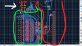
AGND AND DGND
BOTH ARE FULL PLANES TAKING UP THE ENTIRE SPACE OF THE BOARD
COLORED OUTLINES ARE JUST WHERE COMPONENTS WILL CONNECT TO THEIR RESPECTIVE GND'S
TOP LEFT WHITE ARROW IS POINTING TO NET TIE'S CONNECTING ANALOG AND DIGITAL GROUND ONLY IN THAT AREA OF THE BOARD
The ic on the top left is my analog power supply stuff, the one on the top right is the digital supply stuff
electrode inputs and array on the left side of board GREEN
MCU connections , spi, digital stuff on right side of the board RED
LAYER 1 = SIGNALS
LAYER 2 = DGND
LAYER 3 = AGND
LAYER 4 = SIGNALS
Attachments
-
 791.1 KB Views: 7


