I assume that this is the same code exactly that worked on the EEPROM and the RTC? If so, I would think there is a hardware problem.
Does sending Start generate an error?
BTW: it is not necessary or desirable to rename the I2C routines for the device. The read and write routines are general purpose in nature and should just be named I2C_Read and I2C_Write. Every time you edit working code you run the risk of breaking it - same for anybody. Once any routine is debugged and its operation is understood, leave it alone and let it work for you.
EXAMPLE: in line 135, it used to force the RW/ bit low using something like (address & 0xfe). Now you specify the address as a fixed address with the RW/ bit == 0. That should work in WRITE but when you try to READ, you will need just the slave address and let the read routine work the RW/ bit. That was already done, debugged and working and now it's gone.
Any compiler warnings to go along with those red icons?
BTW: it is not necessary or desirable to rename the I2C routines for the device. The read and write routines are general purpose in nature and should just be named I2C_Read and I2C_Write. Every time you edit working code you run the risk of breaking it - same for anybody. Once any routine is debugged and its operation is understood, leave it alone and let it work for you.
sorry. I did changes in code because I thought logically I'm doing right. I removed few routines because that was not necessary to achieve current goal.
EXAMPLE: in line 135, it used to force the RW/ bit low using something like (address & 0xfe). Now you specify the address as a fixed address with the RW/ bit == 0. That should work in WRITE but when you try to READ, you will need just the slave address and let the read routine work the RW/ bit. That was already done, debugged and working and now it's gone.
I've doubt I haven't connected channel pins and alert pin yet so could this be a reason for Not acknowledgement address? should I connect alert pin to ground ?
I'm sure there is no problem in code because it's same code I used before for EEPROM and RTC
C:
//
#define _XTAL_FREQ 20000000     // crystal 20MHz

// PIC18F45K80 Configuration Bit Settings
// CONFIG1L
#pragma config RETEN = ON       // VREG Sleep Enable bit (Ultra low-power regulator is Enabled (Controlled by SRETEN bit))
#pragma config INTOSCSEL = LOW  // LF-INTOSC Low-power Enable bit (LF-INTOSC in Low-power mode during Sleep)
// SOSCSEL = No Setting
#pragma config XINST = OFF      // Extended Instruction Set (Disabled)
// CONFIG1H
#pragma config FOSC = HS2       // HS oscillator (high power, 16 MHz-25 MHz
#pragma config PLLCFG = OFF     // PLL x4 Enable bit (Disabled)
#pragma config FCMEN = OFF      // Fail-Safe Clock Monitor (Disabled)
#pragma config IESO = OFF       // Internal External Oscillator Switch Over Mode (Disabled)
// CONFIG2L
#pragma config PWRTEN = ON      // Power Up Timer (Enabled)
#pragma config BOREN = OFF      // Brown Out Detect (Disabled in hardware, SBOREN disabled)
#pragma config BORV = 0         // Brown-out Reset Voltage bits (3.0V)
#pragma config BORPWR = LOW     // BORMV Power level (BORMV set to low power level)
// CONFIG2H
#pragma config WDTEN = OFF      // Watchdog Timer (WDT disabled in hardware; SWDTEN bit disabled)
#pragma config WDTPS = 1        // Watchdog Postscaler (1:1)
// CONFIG3H
#pragma config CANMX = PORTC    // ECAN Mux bit (ECAN TX and RX pins are located on RC6 and RC7, respectively)
#pragma config MSSPMSK = MSK5   // MSSP address masking (5 bit address masking mode)
#pragma config MCLRE = ON      // Master Clear Enable (MCLR Enabled, RE3 Disabled)
// CONFIG4L
#pragma config STVREN = OFF     // Stack Overflow Reset (Disabled)
#pragma config BBSIZ = BB1K     // Boot Block Size (1K word Boot Block size)
// CONFIG5L
#pragma config CP0 = ON         // Code Protect 00800-01FFF (Enabled)
#pragma config CP1 = ON         // Code Protect 02000-03FFF (Enabled)
#pragma config CP2 = ON         // Code Protect 04000-05FFF (Enabled)
#pragma config CP3 = ON         // Code Protect 06000-07FFF (Enabled)
// CONFIG5H
#pragma config CPB = ON         // Code Protect Boot (Enabled)
#pragma config CPD = ON         // Data EE Read Protect (Enabled)
// CONFIG6L
#pragma config WRT0 = ON        // Table Write Protect 00800-01FFF (Enabled)
#pragma config WRT1 = ON        // Table Write Protect 02000-03FFF (Enabled)
#pragma config WRT2 = ON        // Table Write Protect 04000-05FFF (Enabled)
#pragma config WRT3 = ON        // Table Write Protect 06000-07FFF (Enabled)
// CONFIG6H
#pragma config WRTC = ON        // Config. Write Protect (Enabled)
#pragma config WRTB = ON        // Table Write Protect Boot (Enabled)
#pragma config WRTD = ON        // Data EE Write Protect (Enabled)
// CONFIG7L
#pragma config EBTR0 = ON       // Table Read Protect 00800-01FFF (Enabled)
#pragma config EBTR1 = ON       // Table Read Protect 02000-03FFF (Enabled)
#pragma config EBTR2 = ON       // Table Read Protect 04000-05FFF (Enabled)
#pragma config EBTR3 = ON       // Table Read Protect 06000-07FFF (Enabled)
// CONFIG7H
#pragma config EBTRB = ON       // Table Read Protect Boot (Enabled)
// #pragma config statements should precede project file includes.
// Use project enums instead of #define for ON and OFF.

#pragma warning disable 520

#include <xc.h>

#define ADC_ADDRESS_WRITE        0x90 //first 7-bit I2C address with a low R/W bit
#define CONFIG_REGISTER          0x01 // points to Config register
#define MSB_CONFIG_REGISTER      0x84 // MSB of the Config register to be written
#define LSB_CONFIG_REGISTER      0x83 //LSB of the Config register to be written


void Port_Initialized (void)
{
// LATx registers
    LATA =  0x00;
    LATB =  0x00;
    LATC =  0x00;
    LATD =  0x00;
    LATE =  0x00;

//  TRISx registers
    TRISA = 0x00;    // All are output, Unused
    TRISB = 0x00;    // all are output, Unused
    TRISC = 0x18;    // SDA SCL
    TRISD = 0x00;    // all are output, Unused
    TRISE = 0x00;    // All are output, Unused

    ANCON0 = 0x00;    // Set to digital port
    ANCON1 = 0x00;    // Set to digital port
    CM1CON = 0x00;    // Comparator off
    CM2CON = 0x00;    // Comparator off
    ADCON0 = 0x00;    // A/D conversion Disabled
    ADCON1 = 0x00;    // A/D conversion Disabled
    ADCON2 = 0x00;    // A/D conversion Disabled
}

//Initialize I2C in master mode
void I2C_Initialized(void)
{
    SSPSTAT=0x80; //Slew rate control is disabled for Standard Speed mode (100 kHz and 1 MHz)
    SSPCON1=0x28; // I2C Master mode, clock = FOSC/(4 * (SSPADD + 1))
    SSPCON2=0x00;
    SSPADD = 49;
}

// Send an I2C START
// Return 0 if all ok, 1 if bus collision
__bit I2C_Start(void)
{
    BCLIF = 0;        //Clear 'Bus collision" flag
    SEN = 1;          //initiate a START cycle
    while (SEN);      //wait until it has been sent
    return BCLIF;     //return value of BCLIF flag
}

// Send an I2C STOP
void I2C_Stop(void)
{
    PEN = 1;          //initiate a STOP cycle
    while (PEN);      //wait until it has been sent
}

//Receive one byte. ackflag=0 to send ACK, or 1 to send NAK in reply
//Send one byte. Return 0 if ACK received, or 1 if NAK received
__bit I2C_Sendbyte(unsigned char dat)
{
    SSPBUF = dat;
    asm("nop");           //wait a little for R_W to be set
    while (R_W);    //wait until byte sent and ACK/NAK received
    return ACKSTAT;
}


//Return 0 if all OK, 1 if bus error, 2 if slave address NAK, 3 if slave register NAK, 4 if slave data NAK
unsigned char ADC_Write(unsigned char adc_address, unsigned char config_register, unsigned char MSB_config, unsigned char LSB_config )
{
    if (I2C_Start() )   //send a start, and check if it succeeded
        return 1;   //abort if bus collision

    //send the I2C slave address
    if (I2C_Sendbyte(adc_address  & 0xfe))  //
    {
        I2C_Stop(); //if address was NAKed, terminate the cycle
        return 2;   //and return error code
    }
    //send the Config register
    if (I2C_Sendbyte(config_register))
    {
        I2C_Stop(); //if register was NAKed, terminate the cycle
        return 3;   //and return error code
    }

    //send MSB of Config register
    if (I2C_Sendbyte(MSB_config))
    {
        I2C_Stop(); //if register was NAKed, terminate the cycle
        return 4;   //and return error code
    }

    //send the LSB ofConfig register
    if (I2C_Sendbyte(LSB_config))
    {
        I2C_Stop(); //if register was NAKed, terminate the cycle
        return 5;   //and return error code
    }

    I2C_Stop();
    return 0;   //no error
}

void main(void)
{
    unsigned char ADC_Send;
    Port_Initialized ();
    I2C_Initialized();

    ADC_Send = ADC_Write(ADC_ADDRESS_WRITE , CONFIG_REGISTER, MSB_CONFIG_REGISTER, LSB_CONFIG_REGISTER );

    while(1);
}
It looks like you're doing things right so far. Try changing the slave address to 0xa0 (ONLY, don't change any other names etc) and see if the EEPROM ACKs that slave address. That will verify the I2C bus.
That's why I always say to leave working things alone. When you add something that doesn't work, you can always revert to the last thing that DID work to be sure you haven't broken anything. When you do big changes each time, you never know if the problem is in the new chip or if you just broke something else.
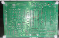
Posting a clear picture of your hookup might help, too.
I am frustrated i don't know what to do. I'm facing a weird problem. I think I still haven't found main problem. Why is it happening that the sometimes old codes I wrote work with the board and sometimes don't?
My first suspect is that there may be problem in my connection. may be loose connection because of bad jumpers wires
I do continuity test to checks each connection with a multimeter. But I have inspected that even after all the connections are fine, my hardware does not work as expected.
Could it be that due to many time pulling of the jumper wire, they would get damaged?
my second suspect is that I am not waiting after enable signal so That's why sometimes the data display on the LCD and sometimes doesn't display. But I am wrong, even after adding nop, the LCD display doesn't show data.
My third suspect is that as the @hexreader told, I should add decoupling capacitor. Can there may be problem because of not having decoupling capacitor on the board.
I know this thread has gone over a three hundred posts. I have got a lot of help. In such situation, To say that my problem is not solved yet. It can hurt to members who are helping me. I'm not trolling I'm telling actual problem that i am facing
I know that you have helped me a lot and I appreciate every help
Usually bad power source and bad connections cause weird erratic behavior if software works ok. For power source ensure:
1. You have sufficient current capability
2. You have good (low ESR) electrolytic capacitor at voltage regulator output (10 to 100 uF)
3. You have decoupling capacitor (about 100nF) near each ICs power inputs.
For connectors ensure:
1. They are not loose
2. Contact surfaces are clean
3. Wires are not started to break at soldering points
Pick ONE thing to test. It could be the LCD, serial, I2C etc but pick one thing.
Load the last code that worked for that device and test it. If it worked once, it has to work again IF the wiring is good AND there are no other problems in the code. It is common for code to appear to work in one test but won't work later if your initialization is incomplete or wrong. I don't know what in particular you are using but if you load it up, test it and post the exact code here, we can help sort it out. Once it is fixed LEAVE IT ALONE and add the next thing. It would be a good thing to put working, tested code for a particular module (like the LCD) in another C source file and include a header file for it in the main code. That way, you can't break it while you are working on another module.
The wiring of course must be perfect. Jumper leads are useful for initial hookups but I like wire and solder. If you can get some small, solid wire to make permanent hookups, you will eliminate the jumper problem.
The chips need to be decoupled for best operation. At the very least, a .1uF ceramic on all power pins to ground on each chip will eliminate decoupling as a possible problem.
Make sure your power supply is solid. Bad power is the root of many problems.
Consider pulling the LCD E line down to ground with a resistor 10K-68K. Sometimes during power up, E can float around before the PIC is initialized causing bad commands to be loaded into the LCD.
That's where I'd start.
Good luck! Glad you're feeling better.
The wiring of course must be perfect. Jumper leads are useful for initial hookups but I like wire and solder. If you can get some small, solid wire to make permanent hookups, you will eliminate the jumper problem.
I have tried many ways to solve the problem by myself. I have already soldered the pins of the LCD directly on the development board. I have soldered the pull UP resistor on small PCB. So I need only few jumper wires
The chips need to be decoupled for best operation. At the very least, a .1uF ceramic on all power pins to ground on each chip will eliminate decoupling as a possible problem
As You Know my understanding for reading PCB layout is very poor. I will need help to connect decoupling capacitor on board. Where do I have to connect the decoupling capacitor,
The board takes 0 to 12 volts AC/DC. I have an regulated adaptor that converts 230 volts into 12V. So the output of this adaptor goes directly to the input of the development board.
Load the last code that worked for that device and test it. If it worked once, it has to work again IF the wiring is good AND there are no other problems in the code. It is common for code to appear to work in one test but won't work later if your initialization is incomplete or wrong. I don't know what in particular you are using but if you load it up, test it and post the exact code here, we can help sort it out. Once it is fixed LEAVE IT ALONE and add the next thing. It would be a good thing to put working, tested code for a particular module (like the LCD) in another C source file and include a header file for it in the main code. That way, you can't break it while you are working on another module.
I really disappointed I don't know why even after working hard, I don't get success. It seems that all the hard work that I was doing till late at night has become waste
But I do appreciate all of you because you are still helping me
I really disappointed I don't know why even after working hard, I don't get success. It seems that all the hard work that I was doing till late at night has become waste
It's more important to work smart. Have a plan and stick to the plan until success.
What module do you want to work on?
Post the EXACT code you have that isn't working and we can drill down into that.
It's more important to work smart. Have a plan and stick to the plan until success.
What module do you want to work on?
Post the EXACT code you have that isn't working and we can drill down into that.
As far as I understand the problem is within hardware, because we have working code that were working before. We just have to find out why it's not working now. For example EEPROM code, post #229, #231
There may be many reasons
First I assume that there can be two main reasons for this.
1) Bad jumper wires
2) decoupling capacitor
1) To check bad connection. I do continuity test with multimeter. I run the code only after confirming all the connections
2) Will it be good idea to add decoupling capacitor on board? Or should I wait for other test? If this is problem where to add decoupling capacitor on the board?
Yes, it sounds like you broke something, especially since none of the previous working codes are now working.
Start at the beginning - does the PIC work? You can find out by loading a simple code (that worked before), setting a breakpoint somewhere early in the code then running under the PK3 debugger. If it hits the breakpoint AND performs a few single steps, the PIC is executing.
If you get that far, keep stepping and see where it fails. It it runs all the way to the last 'while(1)' you at least know the PIC is up and programs will execute.
Step through and ring out the IO.
For example, in the LCD code, set a breakpoint where the E line is high. When it breaks, measure the logic levels on the data bus, R/W and RS to be sure they're correct. Be sure the LCD is powered up.
Once you identify your problem, consider making the wiring permanent. I like using 30ga wire-wrap wire. Since you have .025" square pins on the board, consider wire wrapping your connections. Properly done, wire wrap is as good or better than solder and easily changable with the little twist tools.
Yes, it sounds like you broke something, especially since none of the previous working codes are now working.
Once you identify your problem, consider making the wiring permanent. I like using 30ga wire-wrap wire. Since you have .025" square pins on the board, consider wire wrapping your connections. Properly done, wire wrap is as good or better than solder and easily changable with the little twist tools.
It seems to me that this problem may be happening due to decoupling capacitor. Datasheet recommend few capacitor's but there are no required capacitors on the board.
@JohnInTX I don't understand where to add decoupling cap at the bottom of board
Red marks show VDD pin 11, 32
Black mark show VSS pin 12, 31
10 uF Capacitor's one end will be connected to pin number 6 and the other end will be connected to ground.
Can you tell which is the nearest ground connection to where negative of cap will connect?
?? Pick a known Vss pin and follow the trace.
The picture shows where I would add the 10uF cap to VDDCORE.
ALSO, it looks like power pins 11 and 31 are not hooked to anything. That is BAD. I've shown how I would connect wires to hook them up to the corresponding pins on the other side of the DIP. Both sets of power pins must be hooked up. After adding the wires, add the little decoupling caps as shown above.
Good luck!
If that's all you have it's better than nothing. The datasheet covers exactly what you need, though.
a low-ESR (< 5Ω)
capacitor is required on the VCAP/VDDCORE pin to
stabilize the voltage regulator output voltage. The
VCAP/VDDCORE pin must not be connected to VDD and
must use a capacitor of 10 μF connected to ground. The
type can be ceramic or tantalum. Suitable examples of
capacitors are shown in Table 2-1. Capacitors with
equivalent specifications can be used.
As you use trough hole (leaded) components, then better put tantalum or electrolytic one there. Microchip suggest using low ESR capacitors to core Vdd but i noticed that any capacitor between 10 to 22 uF works.
 Facebook
 Google
 GitHub
 Linkedin