Opinion about PCB routing

Thread Starter

omar-rodriguez

Joined Jun 24, 2015
67
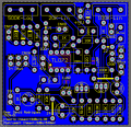
Hi, I just have finished a single sided PCB, it is going to be used in an audio proyect and I just wanted to read some opinions. The PCB has four Jumpers J1, J2, J3 and J4

I know that a bad routing can damage the integrity of the signals but I don't know the techniques to avoid that.

This is the PCB without the ground plane (So you can look at the tracks)

This is the track of the ground

And this is the track of the source

This is the PCB with ground plane

Also.. ¿should the ground plane be on both sides? or just at the bottom layer(the blue one)?
 

Attachments

Willen

Joined Nov 13, 2015
333
As you said it is an audio project, which means low frequency circuit. Low frequency circuit has great chance of working even with the bad pcb design. When you start high frequency circuits like RF related, it needs neat design to work. The RF circuits need proper ground plane, better with double layer of ground plane. So ground plane is not bad. I would keep enough ground plane. It would be fast to etch the board on chemical (if you are going to make it yourself). You have nice skill of PCB design.
 

absf

Joined Dec 29, 2010
1,968
What is the 1uNP next to the 220 resistor? Is it an SMD cap?

If you're mixing SMD with thru hole components, then why not use SMD 100nF near near J1, and place it under the TL072. It would save some place and the PCB will be more neat.
 

SLK001

Joined Nov 29, 2011
1,549
The only thing that I would do would be to make the traces larger. My motto, "Make them as big as you can, but no bigger!" It's free to do and it brings no penalty. What that does is make the resulting board more robust (thin traces are easy to lift off the PCB).

Also, ground plane should be on both sides, if you have a two-sided board - especially for audio. Connect the two planes with plenty of thru vias. A ground plane greatly reduces signal cross-talk.
 

AnalogKid

Joined Aug 1, 2013
10,987
As a general rule, I don't like daisy-chained connections. Example - in the first image, three 10K resistors are connected by one trace. If, during debugging, you need to isolate the bottom pin of the middle resistor, this takes two cuts and one jumper. OTOH if the trace passes below the pin and connects with a short stub, isolating the pin takes one cut and no jumpers.

An even better example is the 10K resistor that is the fifth one over from the right edge and has three traces going into one pad. Isolating that pin requires three cuts and two jumpers, a significant effort.

If space and other design constraints permit, I never run more than one trace to a pad. I learned this the hard way back in the 60's, and it has worked well for me ever since.

Separate from that, consider replacing the component values in the legend with the reference designators, and moving the text out from under the components where it is visible after assembly. This is a *much* more common method of identifying components on a board. Yes, during assembly you have to go back and forth between the assembly drawing and your Bill Of Materials (BOM), but it has two advantages. During debugging, when you want to look at the signal at a certain node, finding it on the board is much easier. Also, if you determine that a component value has to change, the board legend still is correct; only the schematic has to be edited.

Tying these two points together - notice how much easier and less ambiguous my comments about trace routing would be if the board had reference designators on it:

Fifth-resistor-over-from-the-right-edge-of-the-lower-right-corner-of-the-board

becomes

R17.

ak
 
Last edited:
Top