 Facebook
 Google
 GitHub
 Linkedin
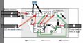
Can the pro's out there look at this simple PCB to tell if there is a fatal flaw or potential flaw in the layout. The circuit is a 3V battery powered LED driver using an ATtiny85 to conserve power wherever possible and to compensate for declining battery voltage by increasing PWM duty cycle. The LEDs will run at very low current, typically < 1mA total. The PCB is designed to be 2- layer and drawn to scale (63mm x 25mm). The attached image shows an overlay of the two layers. Top layer is a ground plane within the gray shape. The bottom layer is traces only, 1mm thick. Black circles are vias to top ground layer, open circles are vias to the bottom trace layer. Power traces are red, signal traces are green, and gnd traces are black. I am worried about ground loops or signal interferences. PCB board is 1oz copper plate and traces will be hand drawn with sharpie. Any comments appreciated.
Attachments
-
 153.2 KB Views: 49


