Facebook
 Google
 GitHub
 Linkedin
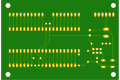
Some unnecessary wire jogs (and 90 degree bends) circled in yellow:I don't know logic of bending wire ? when i feel comfortable i have bend wire at 90 degree and 45 degree in my design

You should avoid 90 degree bends whenever possible.Is there a logic when should wire bend at 45 degree or 90 degree ?