[LTSpice] Help with long tailed pair amplifier

Thread Starter

hrs

Joined Jun 13, 2014
397
Hi,

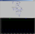
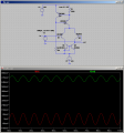
I'm trying to make a long tailed pair input amplifier but I can't get it to work. The attached circuit distorts the input signal and attenuates it. The current source at the top seems to work but there's almost no current going through the current mirror. When I remove the ground from the negative input, all of the current through the current source goes into the emitter of Q3 and out of the base. My guess is I'm applying the input signal incorrectly. Any ideas?

Thanks.
 

Attachments

Thread Starter

hrs

Joined Jun 13, 2014
397
D'oh! I think got confused with NPN versus PNP configurations. After fixing the current mirror there's lots of gain. Thanks!
 

Jony130

Joined Feb 17, 2009
5,488
As a side note,
without current mirror the load current can only swing form 0A to Iee.
1as2.png

But with the current mirror the load current can now swing from +Iee to -Iee (2*Iee) and this is why the voltage gain is now larger.

1as.png

Also do you know why in your simulation the voltage at Q2 collector can only reach voltage around +0.7V?
 

Thread Starter

hrs

Joined Jun 13, 2014
397
As a side note,
without current mirror the load current can only swing form 0A to Iee.

But with the current mirror the load current can now swing from +Iee to -Iee (2*Iee) and this is why the voltage gain is now larger.
Yes, it's very clear from your diagrams.

Also do you know why in your simulation the voltage at Q2 collector can only reach voltage around +0.7V?
I don't think I do. I would have expected it to be lower than the base of Q2 which is at 0V. But with the incorrect mirror there's no current path at the collector of Q2 so maybe it gets pulled up to whatever Q1 is doing + 1 diode drop from the Q1 emitter to base?

In trying to figure out why it wasn't working I came across a discussion (that I can't find anymore) about how a PNP long tailed pair would be lower noise than an NPN one and that the NPN Vas that goed with the PNP long tailed pair would be superior to a PNP Vas ...

Why would a PNP LTP be lower noise that NPN? Are PNP devices generally less noisy? What is a Vas?
 

Jony130

Joined Feb 17, 2009
5,488
I don't think I do. I would have expected it to be lower than the base of Q2 which is at 0V. But with the incorrect mirror there's no current path at the collector of Q2 so maybe it gets pulled up to whatever Q1 is doing + 1 diode drop from the Q1 emitter to base?
Q2 enters saturation region
Why would a PNP LTP be lower noise that NPN?
Lower rbb ? I don't even know if this is true today.
What about if I want to build a full complementary input stage (using both NPN/PNP LTP) ?

And I will quote a Nelson Pass :
" I think that PNP's were and are popular because the original RCA manual used them that way, and they remain vestigial design items"
Are PNP devices generally less noisy?
No
What is a Vas?
Well VAS is a Voltage Amplifier Stage also known as Trans-Impedance Stage (TIS) and typical the VAS is the second stage, usually a Common Emitter (CE) amplifier and the VAS stage needs to provides all the voltage gain and full output voltage swing.
And the input stage with LTP (long tailed pair) is called transconductance amplifier. A transconductance is a voltage controlled current source (differential voltage-to-current converter). Also from what I know only Audio designers will use this type of nomenclature.
 
Last edited:

Thread Starter

hrs

Joined Jun 13, 2014
397
Q2 enters saturation region
Ah, yes I see.

What about if I want to build a full complementary input stage (using both NPN/PNP LTP) ?
Like in figure 15 here? http://sound.whsites.net/ism.htm#p8

Well VAS is a Voltage Amplifier Stage also known as Trans-Impedance Stage (TIS) and typical the VAS is the second stage, usually a Common Emitter (CE) amplifier and the VAS stage needs to provides all the voltage gain and full output voltage swing.
And the input stage with LTP (long tailed pair) is called transconductance amplifier. A transconductance is a voltage controlled current source (differential voltage-to-current converter). Also from what I know only Audio designers will use this type of nomenclature.
Thanks. Today I found VAS mentioned here as well: http://sound.whsites.net/articles/distortion+fb.htm#a2
It seems that an LTP provides a lot of gain so wouldn't a VAS provide additional gain in stead of all the (voltage) gain?

I have a lot of experimenting to do now the basic circuit is working :)

One more thing that I thought of today was how to apply global feedback while keeping the differential input like an opamp. The examples I found all put feedback in one of the two transistors of the LTP leaving only one input signal. But I'll try to figure that out myself first.
 

Jony130

Joined Feb 17, 2009
5,488
No, something like this
Input_stage.png

It seems that an LTP provides a lot of gain so wouldn't a VAS provide additional gain in stead of all the (voltage) gain?
Are you sure about this "a lot of gain" ?? Let me check this
p3a-f1.gif

Q1 and Q2 ---->Ic1 ≈ 0.5 * (VD1 - Vbe3)/R7 ≈ 0.5*(1.6V - 0.6V)/560Ω ≈ 0.5*1.8mA ≈ 0.9mA---->re = 26mV/0.9mA ≈ 29Ω
The VAS current is Ic4 ≈ Vee/(R9+R10) ≈ 35V/6.6kΩ ≈ 5.3mA. Therefore re4 ≈ 26mV/5.3mA ≈ 5Ω
If Hfe (β4) of a VAS transistor is equal to 100 we can find the input stage gain:

Av1 ≈ Rc/(2re) ≈ (R6||(β4*re4))/(2*29Ω) = (560Ω||500Ω)/58Ω ≈ 265Ω/58Ω = 4.6 [V/V] is this a lot of gain ??

And the VAS gain is larger than 6.6kΩ/5Ω = 1320 [V/V] because C5 is a bootstrap capacitor, so R9 is dynamical increased R9' = R9/(1 - Output stage gain), for Output stage gain around 0.8 [V/V] R9' ≈ 5*3.3kΩ ≈ 16.5kΩ

As you can see VAS stage provides the majority of the voltage gain.
 

Thread Starter

hrs

Joined Jun 13, 2014
397
Thanks Jony, I'll need to chew on that for a while.

After fixing the current mirror like you and Alec said I got something like the attached result. Apart from a biasing isue with the output that I need to figure out, it looks like a 2mV p-p to 4V p-p which is a gain of 2000 V/V. So I thought that an LTP provides a lot of gain.
 

Attachments

Jony130

Joined Feb 17, 2009
5,488
Apart from a biasing isue with the output that I need to figure out
Only negative can fix this issue .
it looks like a 2mV p-p to 4V p-p which is a gain of 2000 V/V. So I thought that an LTP provides a lot of gain.
Only in circuit simulation and without any external load this circuit can achieve such a high voltage gain.
Because now the voltage gain will depend on Q6 and Q2 output impedance ro. And in LTspice the early voltage (VAF) for 2N3904 and 2N3906 is 100V (I measured VAF in the bench for 2n3906 and I get 40V) therefore:
ro6 = ro2 ≈ VAF/Ic ≈ 100V/1mA ≈ 100kΩ and the gain is Av ≈ (ro6||ro2)/re2 ≈ 50kΩ/26Ω ≈ 1923 V/V.
Where re = Vt/Ie ≈ 26mV/Ic2 ≈ 26mV/1mA ≈ 26Ω

And in real amplifier VAS stage and Rc is the load for our LTP and this is why the voltage gain is low. But we do not care about it.
 
Last edited:
Top