Hello, I'm working about a DC-AC converter with 400kHz switching frequency. I'm trying to simulate it in Ltspice using the model provided by the manufacturer of the transistor that is a GS66516B by gansystems ( https://gansystems.com/gan-transistors/gs66516b/ ). I want to evaluate power losses and then compare them with measures. I realized a sinusoidal PWM control signal with a dead time of 100ns and the Vgs has a range of -3V / 6V.
Voltage and current on the load are good but I found problems with the source current because there are high peaks and I can't understand why.
This is the model:

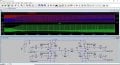
These are the PWM signals and the Vgs: there are fluctuations when the waves have different lenght


And these are Drain currents for first and second switch and source current

What can I do? If you want i can post simulation files. Thanks in advance!
Voltage and current on the load are good but I found problems with the source current because there are high peaks and I can't understand why.
This is the model:
These are the PWM signals and the Vgs: there are fluctuations when the waves have different lenght
And these are Drain currents for first and second switch and source current
What can I do? If you want i can post simulation files. Thanks in advance!