Facebook
 Google
 GitHub
 Linkedin
Hi Eric,
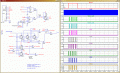
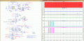
Actually method you shown will also work. But it will be hard to look at one shot. I was looking for if any option where all files can be linked. Like in schematic for multiple pages we are connecting with off page net lines.
Regards,
Amod
Actually method you shown will also work. But it will be hard to look at one shot. I was looking for if any option where all files can be linked. Like in schematic for multiple pages we are connecting with off page net lines.
Regards,
Amod


")