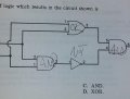
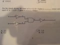
If I have a AND, OR, NOT, and another AND gate, what will be the resulting logic? Seems easy, NAND? Do you need more info or that is enough?
Okay, let's examine the input of A=0 and B=0 first. Both inputs have NOT gates, so you can immediately invert them. So the inputs to the AND gate are 1 and 1. What happens if both inputs to an AND gate are high? The output is.....? Then you invert that to get Z.Another challenge, my guess is circled. Any clue will be greatly appreciated.

Thanks right, NOT gates invert. Makes them pretty easy to understand. So the answer is 1,1.Okay, let's examine the input of A=0 and B=0 first. Both inputs have NOT gates, so you can immediately invert them. So the inputs to the AND gate are 1 and 1. What happens if both inputs to an AND gate are high? The output is.....? Then you invert that to get Z.
Then do the same thing, but with A=0 and B=1.
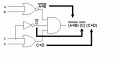
I suggest you copy down the circuit and write the current state on each connection. Like this:
View attachment 47714
Don't hesitate to write down the state after each gate. It will help you keep track of what's going on.
I'd suggest you re-check your logic there. Don't forget there's another NOT gate after the AND gate. And that the X,Y answer system means for condition (a) the answer is X, and for condition (b) the answer is Y.Thanks right, NOT gates invert. Makes them pretty easy to understand. So the answer is 1,1.
I feel I may be kinda not making people happy with these question. Its just that for whatever reason this part, Boolean algebra and gates really gave me fits. This is the only part of the program that gave me this much trouble. Not saying I was Einstein with every part, but this part in particular gave me trouble. Truth tables in particular. Thanks for the help, and I apologize if I aggravated anyone.
It's not really that simple. NAND means that the output is 1 if one or more of the inputs is 0. It's the exact opposite of an AND gate. Look at the following truth tables:OK, thank you! I actually feel like I accomplished something. Now for that same circuit the type of logic created is NAND right, because its NOT and AND together, right?
AND:
A B X
0 0 0
0 1 0
1 0 0
1 1 1
NAND:
A B X
0 0 1
0 1 1
1 0 1
1 1 0
| Thread starter | Similar threads | Forum | Replies | Date |
|---|---|---|---|---|
| R | Help with a CMOS logic gate circuit | Homework Help | 5 | |
| T | Logic gate help | Digital Design | 16 | |
| A | Help with logic gate circuit problem | Homework Help | 13 | |
| V | Logic gate circuit HELP | Homework Help | 10 | |
|
|
Pls help with logic gate | Digital Design | 10 |