Keep Breaking IRS2186 gate drivers (I think)

Thread Starter

jlawley1969

Joined Feb 22, 2021
97
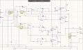
So I am having an issue with my inverter circuit. It was running fine for a long time then I tried it on a different power supply which allowed more current. I assume the current is what broke it but I only put a load on it that would equate to about .5A. For reference I before this point I was testing on a source only capable of .4A. From what I can tell from the data sheet for the Gate driver (https://www.infineon.com/dgdl/irs2186pbf.pdf?fileId=5546d462533600a40153567716c427ed) it should be able to handle 2 or 4 amps either way should have been with in safety margin.

But If I am being honest I do not understand what the data sheet means by "Output high short circuit pulsed current" does that mean the current coming out of the IC to the (in my case) MOSFET's gate? That would make sense to me but it doesnt make sense to me why it would have to be so high to just drive the MOSFET.

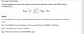
Lastly the reason I think the chip is broken is because it is reading the VCC voltage the High and low INPUT pins which should be either reading the signal I am sending to it or 0 if nothing is attached. but also the chip is taking a good bit more current on the VCC pin like about 0.04A which it did not used to do and is above what data sheet says it should be drawing.
thanks
 

MisterBill2

Joined Jan 23, 2018
18,167
I suggest locating the manufacturer's application notes for the driver and comparing the recommended circuit with your circuit. Also, it may be that some spikes are traveling back from the switching transistors into the driver, and that would cause a failure. inverter circuits can be very challenging.
 

ronsimpson

Joined Oct 7, 2019
2,985
Output high short circuit pulsed current" does that mean
This part is rated for 2/4/6A max. shorted to ground or supply for 10uS and no more. Some people try to use these as motor drivers. The part will get hot and burn out as a motor driver.
The Gate of a MOSFET draws uA at DC. At ac is a capacitor that must be charged up. Say you have 15 ohms Gate resistor, then you start charging up the Gate with about 1A for 25nS.

Post your schematic.
 

Thread Starter

jlawley1969

Joined Feb 22, 2021
97
here is the schematic. What I have here is a most surface mount components listed but I am using comparable through hole components at the moment.

components that I am using now are
attiny13
IRS2186(different pinout from IRS21867)
IRFI644GPBF(but I was going to switch to FDP15N40 because I had previously broken 2 of the prior MOSFETs )
 

Attachments

Irving

Joined Jan 30, 2016
3,843
Remove the 220k pulldown gate resistors, they aren't required and anyway should return to Source not ground on the upper MOSFETs.

The diodes on the series gate resistors are increasing the current in the gate drivers. They aren't needed if your gate resistor is correctly sized. 33ohm is probably not optimal. Read this application note from TI... Layout and minimising drive lengths to reduces parasitic inductances are critical...
 

Thread Starter

jlawley1969

Joined Feb 22, 2021
97
Remove the 220k pulldown gate resistors, they aren't required and anyway should return to Source not ground on the upper MOSFETs.

The diodes on the series gate resistors are increasing the current in the gate drivers. They aren't needed if your gate resistor is correctly sized. 33ohm is probably not optimal. Read this application note from TI...
Ive read that and alot others concerning the gate resistor. It has been extremely annoying and time consuming because I (or rather my company) do not have a proper oscilloscope to measure the frequency of the ringing. I only have a hand held one that shows me the waveform. I have used this calculation but forgot to site the source...

BUT my high sides were floating and so the upper MOSFETs were not closing when they were supposed to, this was when I was actually testing the circuit in the real world. Why should it be pulled to source instead of ground?
thanks
 

Attachments

ronsimpson

Joined Oct 7, 2019
2,985
I would keep the resistor. It must be from Gate to Source!

A MOSFET is turned on by voltage from G to S and does not care where ground is.

If the resistor is causing problems it is because it is discharging C1, C2. (which is small) What frequency? Energy stored in C1 is used to charge up the Gare Capacitance and to hold up the gate for the "on time". The resistor does steel some energy from C1, if connected to Source. If connected the ground there is a very large resistor current which will suck C1 down fast.

Where are the power supply capacitors for U1, U7? The diodes D12, 13 must be "fast".
 

Irving

Joined Jan 30, 2016
3,843
Developing an inverter without a decent 'scope makes it hard work... and expensive as you are discovering... esp as a decent older scope can be picked up for peanuts on eBay, like my 4-channel 100MHz HP from around the 1980s for under $100, though I do have a nice new Siglent 200MHz 4-ch DSO now as well.

Anyway, the 'pulldown' resistor should have no effect on turn off as your driver provides active pulldown to source potential. If it doesn't then you're doing something wrong... but the resistor is affecting your boost potential from C1.

What's the drain voltage on Q1/Q3?
 

shortbus

Joined Sep 30, 2009
10,045
The diodes on the series gate resistors are increasing the current in the gate drivers. They aren't needed if your gate resistor is correctly sized. 33ohm is probably not optimal.
This is something I've come to believe too. But many circuits posted on line always show a diode to "speed up" the mosfet turn off. This may have been the thinking years ago but it's my understanding that the biggest reason to not use them is the gate ringing when the gate resistor isn't used at shut off. But people still see them on web circuits so they just add them to theirs.

Also they tend to use gate resistors of too high a value, I've seen some up or above 1K ohms in circuits, when a better number would be closer to 50ohms for most circuits.
 

ronsimpson

Joined Oct 7, 2019
2,985
First thing is to fix the top Gate resistor to ground. That causes many problems.
Second is to add capacitors on the +5V at the micro. And the Gate drive supply at the gate driver.

The rest if this if for another day.
 

Thread Starter

jlawley1969

Joined Feb 22, 2021
97
Ok first here is another chunk of the circuit
it is a buck converter using the LNK3204D-TL. I have it set up to output ~15volts which it does fairly reliably and with a little noise on the output. So that is what is powering U1/7 as well as U3 via 5V regulator.

Also yes the reason I was using the pull down was because the High side gate signal was going from ON for the period of time it was supposed to then floating at about half the voltage during the dead time before the Low side was triggered. I also believed that the current is supposed to be dissipated through the gate driver according to its block diagram. I had other issue with the high side gate signal but this was the only thing I couldn't attribute to cross talk or poor routing.

Q1/Q3drain voltages are 160VDC
 

Thread Starter

jlawley1969

Joined Feb 22, 2021
97
Ill also look into getting a 'scope but I am hoping my boss agrees to drop this project because I am supposed to fit this in the size of 2 cigarette packs
 

ronsimpson

Joined Oct 7, 2019
2,985
then floating at about half the voltage during the dead time before the Low side was triggered.
Remove the resistor or put the resistor from G to S. Increase the capacitor. 10uF The slower the switching frequency the larger the capacitor value. With this type of circuit you can not leave the top transistor on for a long time.
 

Irving

Joined Jan 30, 2016
3,843
Would be helpful to see whole circuit - hard to assess in little bits as so many things can impact where least expected...
 

Thread Starter

jlawley1969

Joined Feb 22, 2021
97
Sorry I didnt want to post the entire thing because it loses resolution. I am in altium and don't know how to save the schematic as a .tif or something similar.
Also yes my circuit is isolated
 

Attachments

Irving

Joined Jan 30, 2016
3,843
Is this driving the AC output directly or via a transformer that's not shown on schematic?

As far as I can see you have a rectified 120V AC input that generates 160v DC and you have a full bridge driving AC out but no smoothing circuitry so its not clear what you expect the output to look like. Separately there's a buck converter off the 160V DC to generate +15v(?) to power the gate drivers and from that another linear reg to 5v to drive the logic and MCU?
 

MisterBill2

Joined Jan 23, 2018
18,167
As I see that schematic, which has excellent resolution on my screen, it looks like the source connection to the driver is rather complex. If that connection carries other currents then the gate/source voltage may have all kinds of noise, and that certainly can cause voltage spike problems.
 

Irving

Joined Jan 30, 2016
3,843
[...] the source connection to the driver is rather complex
Looks pretty conventional to me, with standard bootstrap diode/capacitor arrangement. You're right about the layout of the source connection being complex though. its important that the hi-side source to low-side drain and the output is separate from the gate-source circulating current. The gate-driver to hi-side source needs to be a kelvin connection independent of the output. Any additional common inductance between source and gate drive can have nasty consequences.

1630599645582.png

layout1.JPG
Here is a bad layout. The high-side gate current return to U1 pin 6 (labelled 'out') is taken off the Q1-source/Q2-drain junction just as shown in the schematic... this means the high current into the load from Q1 through the parasitic inductance of the link to Q2 has a direct impact on the gate current/drive voltage to Q1.
layout2.JPGThis is better. A slight rearrangement and the gate return is taken directly off the Q1 source connection. It still not great though.
1630607669320.pngBetter still. The gate drive return is isolated from any output currents. Gate drives are almost identical lengths, though the low-side could be a tad longer which needs a minor reposition of R2.
 

Thread Starter

jlawley1969

Joined Feb 22, 2021
97
Is this driving the AC output directly or via a transformer that's not shown on schematic?

As far as I can see you have a rectified 120V AC input that generates 160v DC and you have a full bridge driving AC out but no smoothing circuitry so its not clear what you expect the output to look like. Separately there's a buck converter off the 160V DC to generate +15v(?) to power the gate drivers and from that another linear reg to 5v to drive the logic and MCU?
Hi,
I am getting AC via an isolation transformer but it is still 120VAC. I only have those 2 small capacitors for filtering but they are mostly place holders for the PCB as I am using 5.4uF on the prototype board. With no/light load the rectified signal had surprisingly small amount of ripple(obviously this will go up with more load). but yes the rest is correct.

Can you elaborate on the
" You're right about the layout of the source connection being complex though. its important that the hi-side source to low-side drain and the output is separate from the gate-source circulating current."
Are these two sentences related? how is the Source complex? should I be "grounding" the two Sources to each other and thats it? And for the second sentence, is that something I should be doing in the schematic or more so something to do with PCB layout because I do not really understand what I would do to change the schematic.

Thank you for taking the time to show me the proper PCB layout I really appreciate that and all your help thus far.
 
Top