Just some general questions about remaking something from the past

Status
Not open for further replies.

Thread Starter

Berzerker

Joined Jul 29, 2018
623
@ebeowulf17
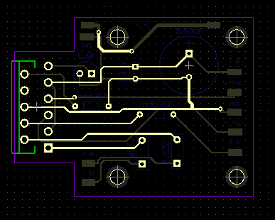
I got the components on the sides I wanted, but the names of them are backwards. Can you change this?
And I looked up how to change trace line width so I tried, nothing changed. it still says .013 thick? I would like .025 to .031.
Do you have to have the top silk printed on the board?
I think the backwards names are from me naming them in the layout so I would know which one was what. I want to remove one silk outline and place others
 
Last edited:
@ebeowulf17
I got the components on the sides I wanted, but the names of them are backwards. Can you change this?
And I looked up how to change trace line width so I tried, nothing changed. it still says .013 thick? I would like .025 to .031.
Do you have to have the top silk printed on the board?
I think the backwards names are from me naming them in the layout so I would know which one was what. I want to remove one silk outline and place others
They are backwards because they will be printed on the bottom of the board.
 

Thread Starter

Berzerker

Joined Jul 29, 2018
623
Sonoran said:
They are backwards because they will be printed on the bottom of the board.
Thanks Sonoran
Maybe it's just me but I think it looks dumb (?) There should be a way to flip it. reminds me of holding something up to a mirror.
@Sonoran Desert Tortoise
I'll soon be purchasing things just to let you know. BUT.... I want to make sure I have everything right before that happens.
I don't want anything going wrong and have to correct it and then re-order. I've been designing in Autocad and then making the parts to reflect what's in the drawing and making sure everything fits and has room. It all has to fit on a 4" x 5 1/2" plate.
 
Thanks Sonoran
Maybe it's just me but I think it looks dumb (?) There should be a way to flip it. reminds me of holding something up to a mirror.
@Sonoran Desert Tortoise
I'll soon be purchasing things just to let you know. BUT.... I want to make sure I have everything right before that happens.
I don't want anything going wrong and have to correct it and then re-order. I've been designing in Autocad and then making the parts to reflect what's in the drawing and making sure everything fits and has room. It all has to fit on a 4" x 5 1/2" plate.
It never works out perfectly the first time, that is why somebody put the "re" in front of the "search".
 

ebeowulf17

Joined Aug 12, 2014
3,307
I got the components on the sides I wanted, but the names of them are backwards. Can you change this?
Do you mean that some parts are mounted on the backside of the board, and those parts' silkscreen labels appear to read backwards on screen? If so, this is perfectly normal and correct. On screen, you're seeing "through" the board as if it were transparent. In real life, you'd have to flip the board over to see the makings, at which point they wouldn't appear backwards anymore.
And I looked up how to change trace line width so I tried, nothing changed. it still says .013 thick? I would like .025 to .031.
There are a few ways to go about setting trace widths. You can set default widths for certain situations, but those will only apply to NEW traces you draw. You can set widths based on which bus/net they're on, but those only take effect if the specific trace width setting is "by net" or something like that, instead of a specific width.

Anyway, for traces that already exist I think you have manually edit them by clicking (maybe right clicking) and changing them per trace. I apologize - this is all from memory, so I my have some details wrong, but hopefully the general idea is right.

Do you have to have the top silk printed on the board?
You don't have to have any silkscreen, top or bottom. You're the designer, so it's up to you. I use silkscreens both top and bottom for work, and top-only when I'm doing small scale personal projects.
 

Thread Starter

Berzerker

Joined Jul 29, 2018
623
I'll let you take a look ebeowulf when I go over everything and double check it.
See the IC's outline. I don't want it on there. I had to do this because of the way I designed it. and I made the pattern up before I placed it in the PCB layout and I don't feel like editing it and going through all that to get rid of it.
 

ebeowulf17

Joined Aug 12, 2014
3,307
I'll let you take a look ebeowulf when I go over everything and double check it.
See the IC's outline. I don't want it on there. I had to do this because of the way I designed it. and I made the pattern up before I placed it in the PCB layout and I don't feel like editing it and going through all that to get rid of it.
I don't quite understand. Do you want any silkscreen markings at all? If not, you can turn the silkscreen layer visibility off so you no longer see it on screen, and you can order PCBs with no silkscreen. It'll still exist as data in the file, but you don't ever have to see it.

I'm not aware of any way to disable the silkscreen for just that part while leaving other silkscreen info intact. If you want to have other silkscreen items, but eliminate just that one, you may have to edit the component pattern again.

If I were in your shoes, I'd edit the pattern and get it right (by right, I mean however you want it - there's no law saying what the silkscreen has to be!)
 

Audioguru

Joined Dec 20, 2007
11,248
If the output power is 25W then the peak current from a 16V supply into a 4 ohms speaker is 3.5A. The heating is about 20W so its current is 1.25A. Then the total peak current to the IC is 4.75A and the traces on the pcb look to be much too narrow for such high current.
 

Thread Starter

Berzerker

Joined Jul 29, 2018
623
ebeowulf said:
I don't quite understand. Do you want any silkscreen markings at all? If not, you can turn the silkscreen layer visibility off so you no longer see it on screen, and you can order PCBs with no silkscreen. It'll still exist as data in the file, but you don't ever have to see it.
I'm not aware of any way to disable the silkscreen for just that part while leaving other silkscreen info intact. If you want to have other silkscreen items, but eliminate just that one, you may have to edit the component pattern again.
If I were in your shoes, I'd edit the pattern and get it right (by right, I mean however you want it - there's no law saying what the silkscreen has to be!)
I'm going to let it go for now. Just part of the IC's silkscreen won't be printed on the board, which I don't really care if it is. this is just for testing and if everything works out then I'll go back and edit it.
AG said:
If the output power is 25W then the peak current from a 16V supply into a 4 ohms speaker is 3.5A. The heating is about 20W so its current is 1.25A. Then the total peak current to the IC is 4.75A and the traces on the pcb look to be much too narrow for such high current.
That's why I was asking AG. They looked too small for me too. I think I'm going with .031 wide. Got to look up how thick I can go on a standard board layout.
Edit: Been trying to look up thickness on traces and I find all kinds of stuff on width but nothing on thickness yet. Can you change this?
 
Last edited:
I'm going to let it go for now. Just part of the IC's silkscreen won't be printed on the board, which I don't really care if it is. this is just for testing and if everything works out then I'll go back and edit it.

That's why I was asking AG. They looked too small for me too. I think I'm going with .031 wide. Got to look up how thick I can go on a standard board layout.
Edit: Been trying to look up thickness on traces and I find all kinds of stuff on width but nothing on thickness yet. Can you change this?
Google "trace width calculator" any you'll get many options to tell you that you'll need 0.080" trace width for a 4A load if using 1 oz/square foot copper PCB.
Here is one, there are many more...
https://www.4pcb.com/trace-width-calculator.html
 

Thread Starter

Berzerker

Joined Jul 29, 2018
623
Sonoran said:
Google "trace width calculator" any you'll get many options to tell you that you'll need 0.080" trace width for a 4A load if using 1 oz/square foot copper PCB.
Here is one, there are many more...
https://www.4pcb.com/trace-width-calculator.html
I found that. But I am limited on how wide I can make them. There is only .097 distance between them. with the rules in place of .013 clearance,
.013 x 2 + .080 = .106 "that's to wide". That's why I'm asking about thickness.
I've been trying to figure out where you change it in diptrace.
 
Last edited:

shortbus

Joined Sep 30, 2009
10,049
Edit: Been trying to look up thickness on traces and I find all kinds of stuff on width but nothing on thickness yet.
Like Sonora said thickness is up to the blank board you choose, ounces of copper. Width is just that how wide your tracks are, you chose this in the board layout. Your board price will go up as you choose heavier copper weight, the price they quoted will probably be for the lightest board.

Got a new idea for you. To get more "power", watts, from the finished speakers, why not use a cross over network and give each speaker it's own amplifier? There will be more than one speaker in each unit won't there?
 

Thread Starter

Berzerker

Joined Jul 29, 2018
623
shortbus said:
Got a new idea for you. To get more "power", watts, from the finished speakers, why not use a cross over network and give each speaker it's own amplifier? There will be more than one speaker in each unit won't there?
each amplifier goes to one speaker, bolted on the bottom. I'm going to go with a 2 ohm speaker "I think".
Still trying to get everything else right shortbus. I have it on my list to look up today but haven't got to it yet.
I can safely go .070 on width but then I'll have to do a lot of correcting and moving things around.
 

shortbus

Joined Sep 30, 2009
10,049
I can safely go .070 on width but then I'll have to do a lot of correcting and moving things around.
After learning to use Diptrace and having you components made, redoing a schematic isn't/shouldn't be that bad. Moving things around will be done by the software, when converting from schematic to PCB. By just setting new track sizes. You did start out with a schematic didn't you? So your not using a teeter and woofer in each one? Seems weird to me if not.

Forgot about this guys page until some one reminded me of it in another post - https://ludens.cl/Electron/Electron.html You might want to look at it and see if some of his amplifier stuff would work for you.
 

Thread Starter

Berzerker

Joined Jul 29, 2018
623
No shortbus "I Cheated" (?) I opened the PCB layout and worked from there. The schematic on the IC's webpage showed me how to hook everything up and I had a layout already made up in AutoCad and I needed to go by it to get the size of the board and all to fit on the back of the plate. the original mindblower amp was only 3 1/4" x 6" long and only about 3/4 thick. There are three PCB's going to be bolted on the back of it, the IC's board and two converters.
But making a schematic up doesn't change the space between the IC's pins.
Yes,I was going to use a triaxial speaker if that's what you were asking.
And AG might be right trying to find a cheap pair of 2 ohm speakers is hard. found a set for about $60.00. not much in the way of Watts though.

Edit; when it says that 1oz. pour is 1.4 mils are they saying it's 1.4 thousands thick?
 
Last edited:
Edit; when it says that 1oz. pour is 1.4 mils are they saying it's 1.4 thousands thick?
Yup. That is why it must be about 80 mils wide to get the cross-sectional area you need. Any narrower and it becomes a resistive heater, turns the board yellow/brown/black, oxidizes the copper traces which causes more resistance, more heat and more damage and that loop continues until it can't get worse, and then it stops.
 
No shortbus "I Cheated" (?) I opened the PCB layout and worked from there. The schematic on the IC's webpage showed me how to hook everything up and I had a layout already made up in AutoCad and I needed to go by it to get the size of the board and all to fit on the back of the plate. the original mindblower amp was only 3 1/4" x 6" long and only about 3/4 thick. There are three PCB's going to be bolted on the back of it, the IC's board and two converters.
But making a schematic up doesn't change the space between the IC's pins.
Yes,I was going to use a triaxial speaker if that's what you were asking.
And AG might be right trying to find a cheap pair of 2 ohm speakers is hard. found a set for about $60.00. not much in the way of Watts though.

Edit; when it says that 1oz. pour is 1.4 mils are they saying it's 1.4 thousands thick?

2-ohm speakers are widely available at your local junk car lot. All kinds of kids from the 80s and 90s put them into 1970s and 1980s cars.
 

Thread Starter

Berzerker

Joined Jul 29, 2018
623
Sonoran said:
Yup. That is why it must be about 80 mils wide to get the cross-sectional area you need. Any narrower and it becomes a resistive heater, turns the board yellow/brown/black, oxidizes the copper traces which causes more resistance, more heat and more damage until it can't get worse, and then it stops.
But you can also make it thicker to take up what you can't go wider with right? as long as there is enough there to handle the load.
 

Thread Starter

Berzerker

Joined Jul 29, 2018
623
Sonoran said:
2-ohm speakers are widely available at your local junk car lot. All kinds of kids from the 80s and 90s put them into 1970s and 1980s cars.
I need new ones. for pricing the unit.
Sonoran said:
Yes, you can pay for 2 oz copper.
found a place that will do 10 for $5.00, that's .50 cents each. even if I have to pay $2.00 0r $3.00 a board it's ok.
 
Status
Not open for further replies.
Top