Facebook
 Google
 GitHub
 Linkedin
Greetings,
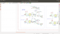
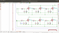
I have been using IXFX180N25T for 3phase Induction motor controller design. The design includes 8 mosfets parallel together. I used a series gate resistor of 1ohm for each individual mosfet after current Booster circuit. Each mosfet has 10K pull down and ceramic cap of 10nf at Gate-source.
Every time one mosfet of high side leg is getting burned, i have provided dead band of 5microsec.
The circuit is mounted on heat sink.I can see some unwanted triggering happening in mosfet.
There is No gate ringing present at No load.
The whole circuits works fine when am using infenion AUIRFP4568.
Kindly let me know if there are some suggestions.