Issue with desoldering usb charging port

Thread Starter

Aaron Peterson

Joined Feb 14, 2018
6
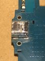
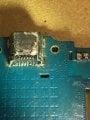
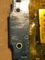
I just recently started getting involved in hobby level electronics repair, and my first project which is repairing a samsung galaxy tab 4 .7.0 micro usb charging port (probably a bit more difficult for a beginner than suggested) I have desoldered as much of the solder around the 4 through holes with a desoldering wick as well as the connectors on the back side of the connector. I am having a hard time getting it to release and it isnt even trying to work loose as of yet. Equipment im using is:

Weller wlc100 soldering station
Tabinger desolder sucker
Tabinfer desoldering wick
Helping hands
Heat tape
A diy type hot air gun using a old sodering gun and aquarium pump (in process of buying a real hot air station)
Electronic flux paste
Various tweezers, etc.

Any tips would be greatly appreciated.
 

bushrat

Joined Nov 29, 2014
209
My method (may not be recommended by everyone) is to flood all contacts with solder, remove the connector (all pins at once) and clean the solder afterwards.
 

ian field

Joined Oct 27, 2012
6,536
After pounding the solder to it how do you heat up everything afterwards?
Most I've seen lately were SMd with the solder pads hidden underneath - you can do it with a rework station.

As I don't have one of those - I usually have to destroy the old connector (very carefully!) - getting the old pins off is then easy. Sometimes its near impossible to hand solder the replacement connector, its just something you have to play by ear.
 

recklessrog

Joined May 23, 2013
985
After pounding the solder to it how do you heat up everything afterwards?
Even though I have several methods of de-soldering, I've used that method many times when needed. Once all the pins are flooded with solder, a wide tipped 75 Watt iron quickly melts the lot and transfers enough heat into whatever is being de-soldered to soften any glue that may have been used to stick it to the circuit board.
Multi pin I.c's that are in soldered through double or multi layer pcb's are best removed buy using a stanley knife or sharp chisel to cut the pins close to the chip body, then remove the pins one at a time. I've had a Denon 300Z desolderer for 20 years that probably is the best you can get, but it's really down to assessing the situation and choosing the most appropriate method for the job in hand. If in doubt of your ability to do it, get some scrap computer or tv boards and practice.
Smd's take a little more finesse with a hot air gun, but even stubborn processors succumb to the leg cut off method. You are less likely to damage the tracks and pads by removing the contact pins one at a time.
 
Last edited:

Thread Starter

Aaron Peterson

Joined Feb 14, 2018
6
I am wondering if there is a solder pad under the actual usb connector that's giving me such a hassle. The 4 through hole pins that hold the connector look like they are flush cut on the back side which doesnt allow me much to work with. Here are a few pictures I have taken to be more definitive.
 

Attachments

ian field

Joined Oct 27, 2012
6,536
I am wondering if there is a solder pad under the actual usb connector that's giving me such a hassle. The 4 through hole pins that hold the connector look like they are flush cut on the back side which doesnt allow me much to work with. Here are a few pictures I have taken to be more definitive.
Looks high risk of torn pads if you try to break the connector up, you could try a heat gun but high risk of blistering the PCB. maybe try draw-filing the top of the tinplate housing and try to get better access to solder holding the pins. Faint possibility you can pry out the plastic b;ock and free the pins one by one. If you can find some way to cut the bottom tinplate - 2 lugs are better to ease out than 4.
 

ElectricSpidey

Joined Dec 2, 2017
3,312
Heh...thru-hole plating...that is a tough nut to crack.

Every time you try to melt the solder it will get harder the next time.

I would use a sharp pair of diagonal cutters and cut the connector up starting across the top, then remove each pin one at a time.
 

recklessrog

Joined May 23, 2013
985
Don't use cutters or you are certain to lift the tracks and pads, buy a very fine modelling metal saw and very carefully make a saw cut right through the top of the metal case (front to back) then saw through the bottom lugs close to but not touching the pcb. then you can open up the top and work on removing the plastic innards, desoldering small bits as you go.
Take your time and don't be tempted to pull hard on anything.
When you fit the replacement, and checked it is working ok, put a thin layer of epoxy resin over where the pins are soldered to take the flexing strain from inserting/removing the usb plug away from the weakened pads, otherwise you are likely to have to repair it again soon.
 
Last edited:

ebp

Joined Feb 8, 2018
2,332
That's a very difficult thing to be starting with. I would find it very difficult & I have lots of experience and lots of special tools. Heat is your friend and temperature your enemy.

As others have suggested, if you can cut the signal pins, that would be a good starting point. It is very easy to rip the pads for them right off the circuit board, so a lot of care is required. A nice $100 pair of cutters is helpful :) A tiny sharp chisel made from some hard steel "music wire" (hobby shop standard item), maybe using a pin vise for a handle, might work to cut the pins one by one at some point where it doesn't transfer stress to the solder pads. The advantage to a chisel over a knife is that you can go at one pin at a time, rocking the chisel side-to-side to cut without applying a lot of pressure. Always think about where that sort of tool will go if it slips. You'll feel bad if you damage the board and silly going to the ER with it stuck all the way through a finger. Xacto makes chisel type blades, but I don't think there are any really small ones.

There is zero (or slightly less) hope of using solder wick for the body. To remove it in one piece you're really going to have to pour the heat in, while assuring that temperature isn't excessive. A pair of hot air tools with suitable nozzles, and possibly some shields to protect adjacent things is what I would try. Lacking two good hot air tools, you might do OK with preheating the bottom with hot air and using a large iron with lots of solder for heat transfer on the top. You are up against a large area of copper on the bottom of the board that has a large number of vias that will conduct heat to top side foil and possibly an inner layer. If you have a replacement connector already on hand, study it for ideas. On some of the connectors I've seen like this, the through-hole tabs are cut out of the part of the metal shell that wraps under the connector. It is very unlikely that the underside of the shell is also surface soldered to the board.

You could go at the connector shell with a rotary ("Dremel") tool with a cutting disk, but that is fraught with peril. If you want to try it, find a way to mask the rest of the board very carefully so you don't get metal dust where you don't want it. Use a vacuum cleaner to keep a strong airflow away from the board and of course be careful to cut so the dust is thrown in the right direction. Did I mention fraught with peril? Again, study a replacement connector and perhaps even sacrifice one to work out the best approach.

One thing I recently ran across on the web is 0.004" (iirc) diameter molybdenum wire. It's sold for cutting apart screens on phones so the glass can be replaced. It's actually electric discharge machining (EDM) cutting wire. I think it is very strong. Fine wire like this can be used to make a loop under an individual lead of a connector or IC to pull it up or just "slice" it from the board when the solder is molten.

There are some very low melting point solders on the market. They can be used to aid removing parts. You remove as much of the ordinary solder as possible, refill with the low temp stuff, and maybe repeat. The lower melting point aids in these situations - or so I hear, I've never tried it. I think the stuff is quite expensive.
 

ElectricSpidey

Joined Dec 2, 2017
3,312
JFTR, I don't think anyone has suggested trying to cut the pins, I know I sure wouldn't try that.

Maybe I wasn't clear, so let me say it a different way...

I would start at the top of the connector snipping a little at a time with a good pair of diagonal cutters, working until there was little left of the connector, and then remove each pin one at a time. (adlib as needed)
 

IamJatinah

Joined Oct 22, 2014
136
Oh my. As others have mentioned, you may already have damage at the fine SMT contacts that lay on the traces. The 4 main lugs you are having trouble with are on a ground-plane which wicks heat from your iron fast. In the future, when desoldering these tender ports, gently preheat that board with a hot air blower you can find at radio shack or the like, which gets hot enough to be uncomfortable, then wick or desolder the joints quickly. I personally always desolder/wick the tiny lap to trace pins first, as reworking the heavy parts will indeed pull traces in a flash. I use hot air then wick pins, then hot air and wick lugs, but don't heat the PCB too much or you will delaminate the layers, cook silkscreens and possibly lift copper. Good Luck.....
 

ebp

Joined Feb 8, 2018
2,332
You can sometimes repair them, depending on how bad the damage is.

If a pad has lifted but is still attached to the track and there is no damage to the board substrate, you can sometimes very carefully glue the pad back in place with a good epoxy. It can be tricky to apply just the right amount.

If a pad is pulled right off, there is adhesive-backed copper foil that can be used for repair, but again it is not easy with such small features. Surface foils on many consumer products runs in the range of about 0.0007" to 0.003" thick. Sometimes you can use a small piece of fine wire (silver plated 30 AWG wire-wrap wire with the insulation stripped is often good, but even that is too heavy in some cases (it is 0.010" in diameter and many SMD tracks are down to about half that in modern stuff), to go directly from a component's pin or terminal to the foil the lost pad connected to. You need to scrape the solder mask from the trace the pad connected to so you can solder the wire. I like a #15 scalpel blade for doing that. If there is no real length of track but the pad connected to a via to an inner layer and the via isn't damaged, there is some hope. If the via is mangled it may be nearly impossible to make a repair. Pulling the copper "barrel" out of a through-hole on a multilayer board is a very bad thing to do. This is a risk you run with the mounting tabs on the connector you are trying to remove if you try to pry up the connector without having the solder completely removed or molten. Pulling the plating out of one or two of the holes for the tabs is a bad thing, but probably not a complete disaster because all four of them most likely make connection to all grounded foils that may exist on inner layers.

An assortment of tweezers is helpful. Good tweezers are fairly expensive. Some of the inexpensive ones from China are quite good, some are very soft steel and complete garbage. Erem's "economy" line, mostly made in Pakistan, isn't too bad. Most of the tweezers I use for electronics run in the range of about $5 to $20, but you can spend a hundred bucks or more on a pair if you're so inclined. One drop onto a hard floor can destroy them.

A headset magnifier or stereo microscope can be a big help. I long wanted a pair of surgeon's binocular telescopic magnifiers, but since I've pretty much packed in doing electronics (partly because my plastic eyes are fixed-focus), I will probably never acquire any. They are quite expensive but have the advantage of substantial working distance, whereas ordinary headset magnifiers give you little unless the magnification is very low. Microscopes vary in working distance, but usually it isn't especially generous. I bought my headset magnifier at a local supplier to the jewelry making art (good source for lots of small tools, including small steel and carbide burrs for rotary tools at much better price than Dremel stuff, but all with 3/32" shafts). I have a very nice Leica microscope, with a really great bench mount, which I got used for just a thousand dollars - a friend ran across them for sale when some business was shutting down.

On hot air tools: I have one that is normally used with nozzles that shape air flow. I sometimes use if without a nozzle. The end of the barrel is about 18 mm / 3/4" OD. I discovered that without a nozzle the air temperature was very non-uniform near the end of the barrel. Adding a barrel extension of thin brass sheet from the hobby shop greatly improved the uniformity of air temperature at the exit. A small thermocouple probe is useful for measuring air temperature at the actual working point. A stand to hold the hot air tool is helpful when you need all four hands to do other things. Silliness aside, learning to hold two things with one hand is a good thing - e.g. holding soldering iron with thumb, 3rd & 4th fingers and feeding solder with 1st & 2nd fingers - not real useful for SMD work, but very useful when soldering wires to connectors & the like
 

Thread Starter

Aaron Peterson

Joined Feb 14, 2018
6
I am quite competent most of the time but I may have gotten in over my head with this project, so much i didnt realize was at stake vs watching a pro on youtube make it fall off
 

IamJatinah

Joined Oct 22, 2014
136
That type of connector gives me the business as well, and I have been IPC certified for over 2 decades. Don't feel bad. Also, Don't bother with copper trace replacement strips, try instead, very fine braided wire, strip about 1" and carefully pull strands out of the multi-stranded you stripped, and tenderly solder tiny wires to contacts. They must be secured, and will easily rip free. Tenderly....like a doctor ;o) Preheating PCB's is handy.
 

ebp

Joined Feb 8, 2018
2,332
I totally agree with IamJatinah. Don't feel bad! It is a difficult task even with lots of experience and the right tools.

One thing I'm curious about is how the connector was soldered to the board in the first place.
The signal pins would be re-flow soldered in a conveyor oven with preheat zones, reflow zones and controlled cooling zones. The body tabs might have be reflowed, but putting solder paste into through holes of that size using the same screen printing methods as for the rest of the board isn't likely to work very well. Sometimes SMD boards go through a wave soldering process for through-hole parts, but if there are SMDs on the back, that has issues. There are machines that will essentially wave solder one pad at a time. In any case, getting the thing on the board in the first place required some planning and extra work.

As you carry on doing this sort of thing you will run into the occasional board where SMD parts have been wave soldered. The parts are glued on first, so they don't come off in the wave. This also makes removal extra painful. You can often spot such boards because tiny blobs of glue, often red, can be seen where it oozed out a little near the middle of components like resistors and capacitors.

Practice on junk. Don't give up. Good luck!
 
Last edited:

IamJatinah

Joined Oct 22, 2014
136
Process flow of paste soldering, SOHO (selective soldering), Convection and Forced Air ovens, and yep, even short active solder pots all play a role in "building" a PCB at the factory. Last factory I was at was 2yrs back at an FDA medical, ASIC, auto-test, assembly plant that made many kinds of boards and assemblies, including LED placements on aluminum substrates, and after over two decades of manufacturing tight-pitched to high power electronics, that LED placement was one of the most interesting, with a lot of Nitrogen cooling jets in the ovens themselves selectively cooling passing assemblies while the substrate nears 1050f. Ovens and profiles of several ovens in series does wonderful things. The Glue mentioned is serious stuff. Placed for decades by pin-head sized needles on x-y beds that held the panels before entering the pick-and-place machines that laid down 3000pcs a minute like a sewing machine on steroids, dots of red glue, held SMT parts in place while one "side" was populated and/or run thru light-driven ovens, stackers would then "flip" the assemblies and in they went into the next oven to cook the other side or placement section. That system has been surpassed, but high volume, fast-paced electronics is a world of wonder in real life ;o)
 
Top