Facebook
 Google
 GitHub
 Linkedin
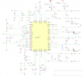
Hi everyone ,I am working on a custom PCB using the TI LM5170QPHPRQ1 as a single-channel buck converter. The design converts 30V input to 12V output at 5A. I am using only Channel 1 ,Channel 2 is unused. Despite trying many fixes the IC is not switching and I am not getting the output voltage please help to make this IC functional below is specifications of the IC .
VIN = 30V (Port A)
VOUT = 12V (Port B)
I_fullscale = 5A
Duty cycle = 12/30 = 0.40 (40%)
f_sw = 100kHz (RT = 40kΩ to GND)
VCC / VCCA = 10V
Mode = Single channel buck (Ch1 only)
Current pin voltage readings
Component values used
RT (OSC) = 40kΩ → 100kHz confirmed from datasheet
SS capacitor = 1µF to AGND
Inductor = 15µH per phase (PQ2614BLA-150K)
Sense resistors = 5× 1mΩ in series = 5mΩ total per phase
OVPA = 120K ohm
OVPB = 120K ohm
COMP network = R=10kΩ, C1=10nF, C2=0.1µF (topology under review)
ISETA = 1.1V DC applied
EN1 = 3.3V (HIGH) ✓
EN2 = GND ✓ (Ch2 disabled)
DIR = HIGH ✓
ISETB = GND ✓
IOUT1,IOUT2 = 5.22V
FAULT = HIGH (10kΩ pull-up to VCC) ✓
VIN = 30V (Port A)
VOUT = 12V (Port B)
I_fullscale = 5A
Duty cycle = 12/30 = 0.40 (40%)
f_sw = 100kHz (RT = 40kΩ to GND)
VCC / VCCA = 10V
Mode = Single channel buck (Ch1 only)
Current pin voltage readings
| Pin | Measured voltage | Expected | Status |
|---|---|---|---|
| VCC | 10V | 8–14V | OK |
| VCCA | 10V | 8–14V | OK |
| OVPA | 0.88V | <1.185V | OK |
| OVPB | 0.11V | <1.185V | OK |
| BRKG | 12.2V | ~VCCA+SW | OK |
| BRKS | 6.14V | ~VCCA+SW | Asymmetric |
| HO | 4.8V static | Switching | Not switching |
| LO | 0V | Switching | Not switching |
| SS | 0V | 0→1.185V ramp | Never charges |
| COMP | 0V | 1.5–2.5V | No voltage |
| OSC | 1.18V | ~1.185V | OK |
| ISENA+/− | 4.5V both | Equal (no current yet) |
RT (OSC) = 40kΩ → 100kHz confirmed from datasheet
SS capacitor = 1µF to AGND
Inductor = 15µH per phase (PQ2614BLA-150K)
Sense resistors = 5× 1mΩ in series = 5mΩ total per phase
OVPA = 120K ohm
OVPB = 120K ohm
COMP network = R=10kΩ, C1=10nF, C2=0.1µF (topology under review)
ISETA = 1.1V DC applied
EN1 = 3.3V (HIGH) ✓
EN2 = GND ✓ (Ch2 disabled)
DIR = HIGH ✓
ISETB = GND ✓
IOUT1,IOUT2 = 5.22V
FAULT = HIGH (10kΩ pull-up to VCC) ✓