Facebook
 Google
 GitHub
 Linkedin
Hello again,What is gm? It is the small-signal transconductance of the device.
What is the small-signal transconductance of the device? It is the rate of change of the current at one port due to a change in voltage at another port. In other words, di/dv where the i and v are at different ports (otherwise it's not a 'trans' conductance, but merely a conductance.
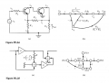
For a BJT, we focus on
di_E/dv_BE
and we define this to be g_m.
The very notion of the small-signal transconductance stems from a desire to be able to linearize the device's behavior so that we can utilize all of the very powerful analysis and design techniques that we have developed for linear systems. So we choose to operate the device with a (normally constant) large-signal bias and apply a time-varying information signal on top of it that is small enough so that the actual response of the device can be adequately approximated by a straight line passing through the large-signal operating point and having a linear response that matches the slope of the device's actual response at that point.
Therefore, the concept of g_m is completely independent of any particular device -- it is mathematical construct that is defined so as to be useful when applying a particular analysis and design technique.
Now, the actual value of g_m for a given device is very much determined by the constitutive relations for that device, which are in turn dictated by the physics that establish those relations.
But we don't have to know or understand anything about the underlying physics, all we need is a mathematical model for them. That model could (and in some cases has and in others still does) come purely from curve-fitting to empirical data. In the case of the BJT transistor, the work in the 1950s was based on understanding the device physics and, my understanding is that, the exponential Ebers-Moll model arose from that. But today, the device physics of integrated transistors is so complex, and the level of fidelity that we need in our models so great, that we don't even attempt to develop models based on device physics; instead, we simply characterize the bejesus out of them and do tons of high-order and piecewise continuous polynomial curve fitting. Our simulators, however, still simply apply this same notion of the mathematical concept of the small-signal transconductance when it comes time to do any simulation that relies on it (such as transfer function sweeps across a frequency range).
I am not sure what you are saying here. What you have been talking about is a behavioral model, which is modeled after the behavior of the device. A physical model contains information about the physical size of the device inside the package and is considered a closer match to a real device.
Now if you do a physical model we will always have dimensions inside there. I dont see how you can get around that but you can explain if you want to.
As you must know, for a mosfet there is W/L i believe that defines gm. So if you define gm that way you can get around the dimensions but you wont be able to define another gm without knowing W and L for the new device.
")