 Facebook
 Google
 GitHub
 Linkedin
input resistance
- Thread starter Сергей999
- Start date
Scroll to continue with content
Jerry-Hat-Trick
- Joined Aug 31, 2022
- 830
I'm thinking, English is probably not your first language as your question is hard to understand. By Emiiter repeater, do you mean emitter follower? And when you say "input current passes through the re " perhaps you mean be - that's base emiiter?
When you apply a voltage to the base of a BJT (bipolar junction transistor) the base emitter acts like a diode so if current flows from base to emiiter of an NPN transistor the emitter voltage will follow the base voltage but be about 0.6 volts lower. hfe (where the "fe" should be in a smaller font than the h, which I can't do here) is the symbol for the gain of the transistor whereby a small base emitter current can control a larger current through the collector by a factor of hfe.
Not a very rigorous explanation, and it's best explained by an example, but is this the question you are asking?
If i understand your question correctly, and i am not sure i do because it is so brief, then this may give you some idea what is going on. I assume you are referring to the calculation of the input resistance of a common emitter circuit.Emitter repeater.
The input current passes through the re, and since the re is nonlinear, we multiply it by h21.
And why do we multiply the Re by h21?
When the transistor gets an input current the collector current goes up by a factor of Beta (simplistically of course). Because the collector current increases by a factor Beta that means the voltage across any internal or external re or Re increases MORE than it would with just the base current alone. This means it makes it easier to raise the emitter voltage with a base current than it would be without the collector current. That means that a smaller base current makes the emitter voltage rise more, and we know that if a small current raises the voltage by more, then the equivalent resistance must be higher (based on Ohm's Law). So the equivalent resistance looks larger so we can account for that by considering that the resistance was higher to begin with and then without actually considering the collector current.
Note that if we disconnected the collector from the circuit the resistance would look like it's actual resistance then, NOT any higher.
So this helps a little sometimes because we dont have to consider the collector current just the Beta and the actual real life emitter resistance(s) to get an estimate of the input resistance.
You can easily experiment with this in a spice simulator using DC analysis.
With say Re=10 Ohms and re=0 (easy to set up with a current controlled current source) if you had the collector open (collector current=0) the input resistance would look like 10 Ohms, but with the collector not open the current source would provide current through Re also, so if Beta=50 then the extra current passing through Re would raise the voltage across the 10 Ohm resistor and so the input resistance would look more like 50*10=500 Ohms. The voltage actually goes up by a factor of Beta+1 but we often just consider it to be Beta because the Beta is usually high enough to ignore the small extra '+1' and after all it's an estimate anyway so there is not really much reason to complicate the factor (even a little) when it's not exact anyway.
May I give you an advice?
Please, use words (as a discription of parts) because it is not quite clear what you mean with symbols like "re" and "Re".
However, I can guess what you mean.
* The resistance of the base-emitter path is h11=hfe=vbe/ib=(ic/gm)/(ic/h21)=h21/gm=h21*re (with gm=1/re)
Note that the transconductance is gm=ic/vbe and h21=beta)).
* When there is an emitter resistor Re it provides negative feedback and increases the total input resistance.
Because the current through Re is not only the base current but - in addition - the collector current (Ie=Ib+Ic) the resulting emitter current is larger than the base current by a factor of h21=beta.
Therefore, the resistor appears larger by the same factor when seen from the input.
Thus, total input resistance is r_in=(h11 + h21*Re)=h21(re + Re)
Last edited:
Read this explanation from LvW again. It answers your question.Because the current through Re is not only the base current but - in addition - the collector current (Ie=Ib+Ic) the resulting emitter current is larger than the base current by a factor of h21=beta.
Therefore, the resistor appears larger by the same factor when seen from the input.
Are you talking about RE (upper case) or about re (lower case)?The essence of the question is that it is difficult to physically imagine how a permanent emitter resistor dynamically reduces its resistance by a factor of h21?
The value of the external RE does not change, but the value of internal re does change with temperature and emitter current and is often taken to be equal to VT/Ie where VT is the thermal voltage often taken to be 26mv. Obviously it changes when Ie changes so that's quite dynamic. It is due to the physical construction of the transistor and the way the diffusion process works. You'd have to look into solid state physics to learn more about that.
Both RE and re provide a pseudo negative feedback which is a little different than true negative feedback but is an interesting way to look at the behavior nonetheless.
If you are talking about the appearance of a changing resistance because of the effect of Beta on the input resistance, that's easy to imagine because the current gain makes the input resistance look higher as mentioned before. The simplest view is:
Rin=(Beta+1)*RE
and you can add re with RE first or use it separately as Beta*re with (Beta+1)*RE to get the total Rin.
As long as you accept the Ebers-Moll model, there is no need to delve any deeper into solid state physics, the construction of the transistor, or the way the diffusion process works.Are you talking about RE (upper case) or about re (lower case)?
The value of the external RE does not change, but the value of internal re does change with temperature and emitter current and is often taken to be equal to VT/Ie where VT is the thermal voltage often taken to be 26mv. Obviously it changes when Ie changes so that's quite dynamic. It is due to the physical construction of the transistor and the way the diffusion process works. You'd have to look into solid state physics to learn more about that.
EBERS-MOLL
\(
i_E \; = \; I_{ES} \left( e^{\frac{v_{BE}}{V_T}} - 1 \right)
\)
If v_BE >> V_T, we can ignore the -1
\(
i_E \; = \; I_{ES} \left( e^{\frac{v_{BE}}{V_T}} \right)
\)
With this model, the result that re = VT/Ie falls directly from the notion that the total response can be reasonably approximated by the superposition of a large-signal and a small-signal response.
Express v_BE as the sum of a large signal and a small signal:
\(
v_{BE} \; = \; V_{BE} \; + \; v_{be} \\
i_E \; = \; I_{ES} \left( e^{\frac{V_{BE} \; + \; v_{be}}{V_T}} \right) \\
i_E \; = \; I_{ES} \left( e^{\frac{V_{BE}}{V_T}} \right) \left( e^{\frac{v_{be}}{V_T}} \right)
\)
If we define I_E to be the current due to V_BE, we get:
\(
v_{BE} \; = \; V_{BE} \; + \; v_{be} \\
I_E \; = \; I_{ES} \left( e^{\frac{V_{BE}}{V_T}} \right) \\
i_E \; = \; I_E \left( e^{\frac{v_{be}}{V_T}} \right)
\)
If v_be << V_T (which defines what is required for it to be "small signal"), then we can leverage
\(
e^x \; \approx \; 1 \; + \; x
\)
To get
\(
i_E \; = \; I_E \left( 1 \; + \; \frac{v_{be}}{V_T} \right)
i_E \; = \; I_E \; + \; I_E \left( \frac{v_{be}}{V_T} \right)
\)
If we define this to be
\(
i_E \; = \; I_E \; + \; i_e
\)
we have
\(
i_e \; = I_E \left( \frac{v_{be}}{V_T} \right) \\
i_e \; = \frac{v_{be}}{\left( \frac{V_T}{I_E} \right) }
\)
Which we can write as
\(
i_e \; = \frac{v_{be}}{r_e}
\)
By defining
\(
r_e \; = \frac{V_T}{I_E}
\)
May I place a short comment on this?Both RE and re provide a pseudo negative feedback which is a little different than true negative feedback but is an interesting way to look at the behavior nonetheless.
I don`t think that we can say that "re" would provide "pseudo negative feedback".
The problem with the expression "re" is that it can be mixed with the external resistor Re - and that is the reason I refuse to use this symbol.
In fact, the quantity "re" is not a resistance - it has just the unit "Ohm" because it is nothing else than the inverse of the transconductance (re=1/gm).
Therefore, the expression re=VT/Ie is derived from the voltage-control characteristic Ie=f(Vbe) - as explicitely shown by WBahn`s excellent contribution.
In contrast, the resistor Re provides "true" negative feedback because it produces a rising voltage V_emitter (when Ic resp. Ie rises) and, thus, reduces Vbe correspondingly.
As long as you accept the Ebers-Moll model, there is no need to delve any deeper into solid state physics, the construction of the transistor, or the way the diffusion process works.
EBERS-MOLL
\(
i_E \; = \; I_{ES} \left( e^{\frac{v_{BE}}{V_T}} - 1 \right)
\)
If v_BE >> V_T, we can ignore the -1
\(
i_E \; = \; I_{ES} \left( e^{\frac{v_{BE}}{V_T}} \right)
\)
With this model, the result that re = VT/Ie falls directly from the notion that the total response can be reasonably approximated by the superposition of a large-signal and a small-signal response.
Express v_BE as the sum of a large signal and a small signal:
\(
v_{BE} \; = \; V_{BE} \; + \; v_{be} \\
i_E \; = \; I_{ES} \left( e^{\frac{V_{BE} \; + \; v_{be}}{V_T}} \right) \\
i_E \; = \; I_{ES} \left( e^{\frac{V_{BE}}{V_T}} \right) \left( e^{\frac{v_{be}}{V_T}} \right)
\)
If we define I_E to be the current due to V_BE, we get:
\(
v_{BE} \; = \; V_{BE} \; + \; v_{be} \\
I_E \; = \; I_{ES} \left( e^{\frac{V_{BE}}{V_T}} \right) \\
i_E \; = \; I_E \left( e^{\frac{v_{be}}{V_T}} \right)
\)
If v_be << V_T (which defines what is required for it to be "small signal"), then we can leverage
\(
e^x \; \approx \; 1 \; + \; x
\)
To get
\(
i_E \; = \; I_E \left( 1 \; + \; \frac{v_{be}}{V_T} \right)
i_E \; = \; I_E \; + \; I_E \left( \frac{v_{be}}{V_T} \right)
\)
If we define this to be
\(
i_E \; = \; I_E \; + \; i_e
\)
we have
\(
i_e \; = I_E \left( \frac{v_{be}}{V_T} \right) \\
i_e \; = \frac{v_{be}}{\left( \frac{V_T}{I_E} \right) }
\)
Which we can write as
\(
i_e \; = \frac{v_{be}}{r_e}
\)
By defining
\(
r_e \; = \frac{V_T}{I_E}
\)
If you want to know more about this you have to look at the dimensions of the transistor and some ideas from solid state physics. Of course once you choose a model you assume you dont need that.
Yes but negative feedback has other attributes that are not expressed simply by one mechanism in theory.May I place a short comment on this?
I don`t think that we can say that "re" would provide "pseudo negative feedback".
The problem with the expression "re" is that it can be mixed with the external resistor Re - and that is the reason I refuse to use this symbol.
In fact, the quantity "re" is not a resistance - it has just the unit "Ohm" because it is nothing else than the inverse of the transconductance (re=1/gm).
Therefore, the expression re=VT/Ie is derived from the voltage-control characteristic Ie=f(Vbe) - as explicitely shown by WBahn`s excellent contribution.
In contrast, the resistor Re provides "true" negative feedback because it produces a rising voltage V_emitter (when Ic resp. Ie rises) and, thus, reduces Vbe correspondingly.
What you say about the negative feedback here is partly true, but misses some points about negative feedback. For example, negative feedback reduces output impedance but that's not happening here. If you look at a simple op amp circuit you will see that with negative feedback the output 'looks' as if it has lower impedance because of the automatic correction of the output signal. If the output was supposed to be 2 volts and with load it dropped down to say 1.9 volts, the negative feedback would (with enough gain of course) bring it back up to 2 volts or nearly so. That's in conjunction with the mechanism you are talking about which has an effect on the INPUT resistance only.
So true negative feedback has other mechanisms at work.
The concept of re (and rpi and gm and...) don't come from solid state physics. Those concepts originate from and are based on the concept of small-signal linearization of the mathematical model of the device. That mathematical model's origin is quite irrelevant -- it could come from theory or be derived purely from empirical observations.If you want to know more about this you have to look at the dimensions of the transistor and some ideas from solid state physics. Of course once you choose a model you assume you dont need that.
Sorry to say - but I disagree with the above. Let me explain:Yes but negative feedback has other attributes that are not expressed simply by one mechanism in theory.
What you say about the negative feedback here is partly true, but misses some points about negative feedback. For example, negative feedback reduces output impedance but that's not happening here. If you look at a simple op amp circuit you will see that with negative feedback the output 'looks' as if it has lower impedance because of the automatic correction of the output signal. If the output was supposed to be 2 volts and with load it dropped down to say 1.9 volts, the negative feedback would (with enough gain of course) bring it back up to 2 volts or nearly so. That's in conjunction with the mechanism you are talking about which has an effect on the INPUT resistance only.
So true negative feedback has other mechanisms at work.
A resistor Re provides "Current-controlled negative Voltage feedback" - and the observed behaviour of the circuit fulfills ALL properties of "true" negative feedback:
* Input resistance goes up (feedback signal is voltage)
* Output resistor goes up (control signal is current)
* Linearity improves
* Signal gain reduces
* Bandwidth increases
* Sensitivity of the closed-loop to active parameter tolerances is drastically reduced (reason for including Re).
Comment to the opamp example: System theory requires that the output resistance increases for curent-controlled feedback (present case) whereas it decreases for voltage-controlled feedback (opamp).
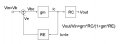
Here is a block diagram which can illustrate the feedback provided by Re. For simplification I have set Ie=Ic (to show the gain reduction caused by the loop gain LG=-gmRe). This closed-loop gain expression is in full accordance with classical feedback theory.

Attachments
-
 17.7 KB Views: 0
Last edited:
Well - I will not (and I cannot) discuss solid state physics here, but the transconductance gm (as the key parameter for the voltage gain properties of a BJT) is directly derived from the BJT`s voltage-control function Ic=f(Vbe/VT) - gm is the slope of this curve at the selected DC operating point.The concept of re (and rpi and gm and...) don't come from solid state physics. Those concepts originate from and are based on the concept of small-signal linearization of the mathematical model of the device. That mathematical model's origin is quite irrelevant -- it could come from theory or be derived purely from empirical observations.
Therefore, I think this characteristic shows the basic properties (function) of the BJT and has, of course, some relation to solid state physics (William Shockley) , does it not ?
So I think, this parameter gm is not "based....on the mathematical model of the device" - in contrast, this model was developed on the basis of the voltage-current relation of the device (expressed by gm).
Sorry to say - but I disagree with the above. Let me explain:
A resistor Re provides "Current-controlled negative Voltage feedback" - and the observed behaviour of the circuit fulfills ALL properties of "true" negative feedback:
* Input resistance goes up (feedback signal is voltage)
* Output resistor goes up (control signal is current)
* Linearity improves
* Signal gain reduces
* Bandwidth increases
* Sensitivity of the closed-loop to active parameter tolerances is drastically reduced (reason for including Re).
Comment to the opamp example: System theory requires that the output resistance increases for curent-controlled feedback (present case) whereas it decreases for voltage-controlled feedback (opamp).
Here is a block diagram which can illustrate the feedback provided by Re. For simplification I have set Ie=Ic (to show the gain reduction caused by the loop gain LG=-gmRe). This closed-loop gain expression is in full accordance with classical feedback theory.
View attachment 278031
Hello,
Not sure what you are showing here but that block diagram does not show the true nature of the circuit.
For one thing, the output impedance is zero which is not true of any transistor circuit that does not provide true negative feedback. I suppose we are talking about a CE amplifier with external RE as that is the simplest to talk about i think. So the block "RC" provides a zero output impedance which is not right as i am sure you know.
This is a problem because one of the things we would like to show that is due to negative feedback in a true system like this is that the output impedance can be brought down to a very low value often considered to be zero. But using a block to show the output automatically makes the output impedance (output resistance) zero which defeats the purpose of trying to show the output resistance becomes zero due to the negative impedance. In other words, the negative feedback in that circuit never changes the output resistance so even without any "RE" block the output resistance is zero.
I use the terms output 'resistance' and 'impedance' here to be the same because we are talking about low frequency operation or even DC where any reactive part is not going to be part of the impedance, and that keeps it a little simpler to talk about also.
Yes, but if you want to go BEYOND that you have to get deeper into transistor theory. That's all am saying.The concept of re (and rpi and gm and...) don't come from solid state physics. Those concepts originate from and are based on the concept of small-signal linearization of the mathematical model of the device. That mathematical model's origin is quite irrelevant -- it could come from theory or be derived purely from empirical observations.
So - what is wrong ?Not sure what you are showing here but that block diagram does not show the true nature of the circuit.
I do not understand (output impedance zero ?).For one thing, the output impedance is zero which is not true of any transistor circuit that does not provide true negative feedback.
In control theory, it is the purpose of such a block diagram to show how feedback works and to derive the loop gain expression. Such a block diagram must not be confused with a circuit diagram which includes real parts.I suppose we are talking about a CE amplifier with external RE as that is the simplest to talk about i think. So the block "RC" provides a zero output impedance which is not right as i am sure you know.
As an example, the node between the gm block and the RC block shows the current at this point as a "state variable" (and not as a current that is split into two parts going to RC and RE).
Therefore, such a block diagram must not be used for discussing real input and output impedances. This is not the task of the diagram. It can (and should) only be used to make visible the signals which are going round the loop.
In the present case, it serves the purpose to show that Re, indeed, provides "true" negative feedback with all well-known advantages and disadvantages.
Another example: In many books about oscillators you can find block diagrams which show how the loop is closed and under which circumstances the Barkhausen condition can be fulfilled (loop gain determination). But, of course, these diagrams must not be used for deriving any information about the output (source) impedance at that node where the oscillatory signal is provided for furthr processing.
Last edited:
What is gm? It is the small-signal transconductance of the device.Well - I will not (and I cannot) discuss solid state physics here, but the transconductance gm (as the key parameter for the voltage gain properties of a BJT) is directly derived from the BJT`s voltage-control function Ic=f(Vbe/VT) - gm is the slope of this curve at the selected DC operating point.
Therefore, I think this characteristic shows the basic properties (function) of the BJT and has, of course, some relation to solid state physics (William Shockley) , does it not ?
So I think, this parameter gm is not "based....on the mathematical model of the device" - in contrast, this model was developed on the basis of the voltage-current relation of the device (expressed by gm).
What is the small-signal transconductance of the device? It is the rate of change of the current at one port due to a change in voltage at another port. In other words, di/dv where the i and v are at different ports (otherwise it's not a 'trans' conductance, but merely a conductance.
For a BJT, we focus on
di_E/dv_BE
and we define this to be g_m.
The very notion of the small-signal transconductance stems from a desire to be able to linearize the device's behavior so that we can utilize all of the very powerful analysis and design techniques that we have developed for linear systems. So we choose to operate the device with a (normally constant) large-signal bias and apply a time-varying information signal on top of it that is small enough so that the actual response of the device can be adequately approximated by a straight line passing through the large-signal operating point and having a linear response that matches the slope of the device's actual response at that point.
Therefore, the concept of g_m is completely independent of any particular device -- it is mathematical construct that is defined so as to be useful when applying a particular analysis and design technique.
Now, the actual value of g_m for a given device is very much determined by the constitutive relations for that device, which are in turn dictated by the physics that establish those relations.
But we don't have to know or understand anything about the underlying physics, all we need is a mathematical model for them. That model could (and in some cases has and in others still does) come purely from curve-fitting to empirical data. In the case of the BJT transistor, the work in the 1950s was based on understanding the device physics and, my understanding is that, the exponential Ebers-Moll model arose from that. But today, the device physics of integrated transistors is so complex, and the level of fidelity that we need in our models so great, that we don't even attempt to develop models based on device physics; instead, we simply characterize the bejesus out of them and do tons of high-order and piecewise continuous polynomial curve fitting. Our simulators, however, still simply apply this same notion of the mathematical concept of the small-signal transconductance when it comes time to do any simulation that relies on it (such as transfer function sweeps across a frequency range).
Hello again.
Yes - I agree with every sentence. Did I say anything different in any of my posts?
Finally, I like to say the following:
My comment in post#14 referred to your post in post#12. Unfortunately, I registered too late that you had replied to a comment by MrAl. So I have interfered without intention in your discussion - I'm sorry.
Last edited:
Hello again and thanks for the reply,So - what is wrong ?
I do not understand (output impedance zero ?).
Yes i know you dont understand the output impedance problem here.
The problem is, and i think i said this already, is that the transistor circuit has output impedance that is non zero, while your block diagram has output impedance (Vout) of exactly and perfectly zero. That's because a block like that shows the output voltage and no way to show how the load affects the output, unless we of course add some parts.
Namely, an output impedance resistor and a load.
So to understand this better, connect an output resistance in series with the last block on the right (Vout) and then add a load to that. Then observe that as the load resistance decreases, the total output voltage (now at the junction of the two added resistances) decreases and there is not a darn thing the "negative feedback" can do about it. That's unless we add a true negative feedback that actually measures the very output which is now at the junction of the two added resistors.
NOW when we have some decent feedback amount, we will see the output impedance get lower because now the feedback can compensate for the output voltage even with load.
Keep in mind this is going by your block diagram as is, you may be able to draw a different block diagram that makes your point more clear you can look into that. I'd be interested to see that.


