 Facebook
 Google
 GitHub
 Linkedin
If it's not a problem for you sir. Im willing to learn. Even if I will not understand, i will do a more deeper research. I hope i can find at least one book. At least one that could this sort of things. Thank you very much in advanceHello again,
I can see you are a deep thinker and that's good because if you keep at it you will eventually find what you are looking for, if not right now. I too have been bugged by the lack of good, general ways to handle some simple electronic problems and so i went after some of those problems and came up with solutions. The solution to the CE amplifier comes from considering everything at the same time. That means relating one thing to another until you can single out each resistor or other part. Circuit synthesis is the reverse of analysis. Once you know how to analyze you can begin to find was to calculate the different components. You then end up with a process as well as a group of formulas. For a really simple example:
R1=R2+R3
and you dont yet know what R2 and R3 are so how do you calculate R1.
Well, in some cases you dont calculate R1, yet, you just use that R2+R3 in the next equation where you see R1 and then you may end up with a formula for R2 and R3, which is now void of R1, and then you can go back and calculate R1 with no problem.
This is what we can do with the CE amplifier, and it starts with the DC bias point.
The formulas you have presented here are probably all correct. The only missing thing is you have to just think a little bit more and see how to simplify things so much that you end up with an equation for one resistor, or something close to that. Sometimes solutions come out as ratios though, because more than one value for two or more parts may work the same or nearly the same. So then you have to choose one (say resistor) and then calculate the other. So you may choose 1k, 2.2k , etc., then calculate the other resistor.
I can show you a procedure for calculating the resistors for a CE amplifier if you like, it's not all that difficult, but it will be a set of formulas and a procedure how to use them It takes maybe 5 minutes. The only thing is though that i dont think this will answer your more general question of how to go about solving circuits LIKE this as well as this one. That would require you to learn a little more about how to analyze a circuit. Not super difficult either though, but you need algebra and that's all for now.
As to the capacitor values you talked about, the coupling capacitors are chosen for not just one but two reasons. The first is to remove the DC component so you just get the AC signal and that means it does not alter the DC bias point of either circuit being coupled. The second is it has to be of large enough value to be able to pass the LOWEST frequency you need to amplify without too much attenuation. This is actually a simple problem too.
The choice of just using a capacitor solves the first problem: the coupling. That's done.
The choice of value is based on frequency, and so you have to do another little equation for the impedance of the capacitor. The impedance is Z=1/(j*w*C) where 'j' is the imaginary operator. In may cases though you can estimate this as Z=R=1/(w*C) (w=2*pi*frequency). that gives you some idea how it will act with different frequencies.
For example, if we approximate 'pi' as simply '3', we can write:
R=1/(2*3*f*C) which is R=1/(6*f*C)
Now for a frequency 'f' of 100 Hertz we get:
R=1/(600*C)
and solving for C we get:
C=1/(600*R)
and so if we want the capacitor to have low impedance 'R' we make R a low value like maybe 100. That gives us:
C=1/(60000)
and that comes out to about 17uf so we might use a 22uf capacitor.
So there is a logic to it, it just takes a little more effort and some analysis.
If you'd like to see the procedure for biasing a CE amplifier, i can show you that, but it will just be a formula or two, somewhat longer than you've seen so far, that takes into account more of the other components too. You may not understand where this formula came from though, unless you are willing to do a little more analysis, but that just means using a lot of symbolic algebra which modern software does pretty good with ease.
In fact, why dont i show you how to develop a simpler aspect of this process so you can get a better idea how it all comes together. I think you may have actually done some of this already.
I need your help on CE amplifier
- Thread starter PaulEngineer
- Start date
Scroll to continue with content
I have the book named "The Art of Electronics 3rd edition" by Paul Horowitz and Winfield HillPaul, let me first say that I do understand your frustation. But I have a question to you:
From your text, I have derived that you have consulted many many books. Did you notice that in some books the BJT is described and explained as a CURRENT-CONTROLLED device and in some other books as a VOLTAGE_CONTROLLED device?
To me, THIS fact is really frustrating. It is really surprising (and frustrating) that even 70 years after the BJT was introduced two different opinions still exist about the basic working principles of this device.
You can be sure - only ONE explanation is correct: Undoubtly, the BJT is VOLTAGE-CONTROLLED.
The basic relation is: Ic=Is[exp(Vbe/Vt)-1].
And all classical steps for designing BJT based gain stages reflect this fact!
This "Ebers-Moll equation" (derived from Shockleys famous formula desribing the voltage-current relation for any pn junction) is, therefore, implementred in all electronic simulation programs.
There are many examples, explanations, formulas, observations and physical constants which clearly proove that Ic does depend only on the voltage Vbe - and the base current Ib=Ic/B is nothing else than an unwanted side effect. I cannot understand that still there are people who think that a very small current should be able to control a current that is 200 times larger. Even from the energy aspect this is impossible!
Of course, the base current Ib does exist and can be considered during design of the biasing network - but it has no controlling function at all.
All people and books stating that the BJT would be current-controlled cannot present any evidence - it is nothing else than a claim! A formula Ic=B*Ib (derived from Ib=Ic/B) cannot say anything about cause and effect. Of course, this also applies to BJT switching applications. It is simply false to say that a large base current wouls drive the BJT into saturation. A large base current is the RESULT of saturation but never its cause.
Knowing this, it is not a problem to design a CE amplifying stage. And the "secret" consists of "negative feedback" - in most cases an emitter resistor RE is used for this purpose. Negative feedback has the big advantage that the circuit performance (DC bias point, voltage gain,...) has a remarkably reduced sensitivity to the BJT parameters. In particular, it is not too important if your calculation assumes Vbe=0.7 volts or Vbe=0.75 volts ....
(Sensitivity of Ic against this voltage is one of the arguments of the "current-control-party" against voltage control - not really an argument!).
If you want I can list the main steps for designing a CE stage ...it is really not a problem.....
Short summary: It is really not a big problem to design a well-working gain stage....and it is pretty logical to see how and why the relevant formulas are to be applied. HOWEVER - the most important step is to UNDERSTAND HOW THE TANSISTOR REALLY WORKS! Without such an understanding it must be "frustrating" to follow blindly some formulas/relationships which can be found in the literature.
PS: Did you consult also the electronic engineers "bible" ("The Art of Electronics" , Horowitz/Hill) ?
Quote: "But to understand differential amplifiers,......and other important applications you must think of the transistor as a transconductance device - collector current is determined by base-to-emiter voltage" (End of quote).
Hi Paul - just for clarification. I have mentioned this book just as an example which correctly describes the BJT as a voltage-controlled device. This was the only reason. I agree with you that it is not the best knowledge source for a beginner. For my opinion, it is more or less a handbook for technicians and engineers.I have the book named "The Art of Electronics 3rd edition" by Paul Horowitz and Winfield Hill
As I have announced, here is a short listing of 5 design steps :
Step 1: Based on (a) the available supply voltage Vcc and (b) the required/wanted voltage gain Av you must select a collector resistor Rc and a DC quiescent current Ic. In this context, the following formula is essential:
Av= - gmRc (with transconductance gm=Ic/Vt).
(Comment: The transconductance gm desribes the slope of the voltage control function Ic=f(Vbe))
Step2: Use an emitter resistor Re with a value of app. 10% of the Rc value (rule of thumb).
The DC voltage drop on (Rc+Re) should be app. 50% of the available DC supply Vcc. From this we can derive an expresssion which gives a good „feeling“ for the maximum possible voltage gain (ignoring Re as a first guess):
Av= - gmRc= - (Ic/Vt)(Vcc/2)/Ic= - Vcc/2Vt (with app. 2Vt=50mV ).
A gain reduction is always posible using signal feedback (step 5).
Step 3: Using the known DC voltage Ve=Ie*Re (set Ie=Ic) at the emitter and with Vbe=0.7 V the required base voltage is Vb=Ve+0.7V. This DC bias voltage should be created with a simple voltage divider (R1, R2) at the base. You are free to select the resistive niveau of this divider chain but there are some constraints (step 4) .
Step 4: The total input resistance should not be too small (with respect to the properties of the driving signal source) - on the other hand, the resistors should allow a DC current through the chain that is remarkably larger than the expected base current Ib=Ic/B (which goes through the upper resistor R1). It is the goal of this „trade-off“ to enable a „stiff“ base voltage Vb (which does not remarkably depend on the very large tolerances of B - another indication for voltage-control).
As a rule of thumb: Current through R1 is app 10*Ib.
Step 5: The emitter resistor Re (or a part of it) can be bypassed with a capacitor Ce. This is because Re does not provide DC feedback only - at the same time it provides also signal feedback which reduces the gain according to the expression:
Av= -gmRc/(1+gmRe).
When such a gain reduction is not desired the influence of Re on signal properties is eliminated with a capacitor Ce.
Final comment: As you can see, there is not only a simple set of formulas which can/must be used for designing such a gain stage. You still have some freedom during this design phase. This is very important because this gives you the chance to adapt the circuit to some application-specific requirements.
Last edited:
I see.. So if I have a good understanding of what you said, for R1 and R2 we choose the resistors by ourselves, and the total resistance of DC bias should not be too much otherwise the base voltage will decrease to the levels bellow the operating point Q, (meaning the cutoff region where Vce≈Vcc) and at the same time it shouldn't be too small because the base voltage will set the transistor to the saturation point (meaning the saturation region where Vce≈0V for ideal condition of function, and almost 0.2-0.7 volts in reality)? That's the first question.Hi Paul - just for clarification. I have mentioned this book just as an example which correctly describes the BJT as a voltage-controlled device. This was the only reason. I agree with you that it is not the best knowledge source for a beginner. For my opinion, it is more or less a handbook for technicians and engineers.
As I have announced, here is a short listing of 5 design steps :
Step 1: Based on (a) the available supply voltage Vcc and (b) the required/wanted voltage gain Av you must select a collector resistor Rc and a DC quiescent current Ic. In this context, the following formula is essential:
Av= - gmRc (with transconductance gm=Ic/Vt).
(Comment: The transconductance gm desribes the slope of the voltage control function Ic=f(Vbe))
Step2: Use an emitter resistor Re with a value of app. 10% of the Rc value (rule of thumb).
The DC voltage drop on (Rc+Re) should be app. 50% of the available DC supply Vcc. From this we can derive an expresssion which gives a good „feeling“ for the maximum possible voltage gain (ignoring Re as a first guess):
Av= - gmRc= - (Ic/Vt)(Vcc/2)/Ic= - Vcc/2Vt (with app. 2Vt=50mV ).
A gain reduction is always posible using signal feedback (step 5).
Step 3: Using the known DC voltage Ve at the emitter and with Vbe=0.7 V the required base voltage is Vb=Ve+0.7V. This DC bias voltage should be created with a simple voltage divider (R1, R2) at the base. You are free to select the resistive niveau of this divider chain but there are some constraints (step 4) .
Step 4: The total input resistance should not be too small (with respect to the properties of the driving signal source) - on the other hand, the resistors should allow a DC current through the chain that is remarkably larger than the expected base current Ib=Ic/B (which goes through the upper resistor R1). It is the goal of this „trade-off“ to enable a „stiff“ base voltage Vb (which does not remarkably depend on the very large tolerances of B - another indication for voltage-control).
As a rule of thumb: Current through R1 is app 10*Ib.
Step 5: The emitter resistor Re (or a part of it) can be bypassed with a capacitor Ce. This is because Re does not provide DC feedback only - at the same time it provides also signal feedback which reduces the gain according to the expression:
Av= -gmRc/(1+gmRe).
When such a gain reduction is not desired the influence of Re on signal properties is eliminated with a capacitor Ce.
Final comment: As you can see, there is not only a simple set of formulas which can/must be used for designing such a gain stage. You still have some freedom during this design phase. This is very important because this gives you the chance to adapt the circuit to some application-specific requirements.
Second question. Does R1 controls the current flowing through the base, and the R2 somehow keeps the Base Bias voltage at a constant voltage stated by the formula Vbb = Vcc(R2(R1+R2))? I don't know how to explain this question in a better way. I'll try it though. The voltage divider has typically the same current with no load connected to it. But when the divider is connected to the base or any load, a portion of the current will flow to the load. So typically.. It's like we say that R1 and R2 is now in a parallel connection? Because in DC equivalent they are in parallel connection.
Third question. If i will choose in example 15V and a collector current of 2mA, then i need app. Vce of 7.5V both on Rc and Re as a voltage drop (VRc+VRe) how can I be sure that my amplifier isn't clipping the signal but outputting a clean sine wave? Oh just to not forget. Is the clipping mean that the amplifier works close to saturation region or even in a saturation region?
Fourth question. Say Vce is 7.5V as described above. Can't i just add two exactly identical resistors to have the same Voltage drop on both of them, meaning 3.75V on both resistors? Or is it critical for Rc and Re to be in different values?
Fifth question. From the lesson i provided a link above, the capacitor needs to be relatively large to allow frequency as low as 20Hz to pass through it, meaning it should be like 169uF according to the formula 1/(2piRC). So if we take it in consideration, then should be the C2 the capacitor that blocks anything above 20KHz? If in example we have a multistage CE amplifier, then the RC that will block the frequency above 20KHz should be the output capacitor of the last stage? Thank you very much. Im very close to understand at least the basics of the CE amplifier.
I see.. So if I have a good understanding of what you said, for R1 and R2 we choose the resistors by ourselves, and the total resistance of DC bias should not be too much otherwise the base voltage will decrease to the levels bellow the operating point Q, (meaning the cutoff region where Vce≈Vcc) and at the same time it shouldn't be too small because the base voltage will set the transistor to the saturation point (meaning the saturation region where Vce≈0V for ideal condition of function, and almost 0.2-0.7 volts in reality)? That's the first question.
Second question. Does R1 controls the current flowing through the base, and the R2 somehow keeps the Base Bias voltage at a constant voltage stated by the formula Vbb = Vcc(R2(R1+R2))? I don't know how to explain this question in a better way. I'll try it though. The voltage divider has typically the same current with no load connected to it. But when the divider is connected to the base or any load, a portion of the current will flow to the load. So typically.. It's like we say that R1 and R2 is now in a parallel connection? Because in DC equivalent they are in parallel connection.
Third question. If i will choose in example 15V and a collector current of 2mA, then i need app. Vce of 7.5V both on Rc and Re as a voltage drop (VRc+VRe) how can I be sure that my amplifier isn't clipping the signal but outputting a clean sine wave? Oh just to not forget. Is the clipping mean that the amplifier works close to saturation region or even in a saturation region?
Fourth question. Say Vce is 7.5V as described above. Can't i just add two exactly identical resistors to have the same Voltage drop on both of them, meaning 3.75V on both resistors? Or is it critical for Rc and Re to be in different values?
Fifth question. From the lesson i provided a link above, the capacitor needs to be relatively large to allow frequency as low as 20Hz to pass through it, meaning it should be like 169uF according to the formula 1/(2piRC). So if we take it in consideration, then should be the C2 the capacitor that blocks anything above 20KHz? If in example we have a multistage CE amplifier, then the RC that will block the frequency above 20KHz should be the output capacitor of the last stage? Thank you very much. Im very close to understand at least the basics of the CE amplifier.
Hi,
Ok i'll show more information, but just a quick note here.
I dont think you should think about the capacitors just yet. That gives the impression that you can just throw a value at any circuit and it will do what you want. Before you do that you should really know about the input and output impedances. This information lets you choose a capacitor.
For example, if a 10uf cap works with a circuit that has a 1k output load, then if another circuit has a 100 Ohm load the cap would have to be 100uf, and if the load was 10 Ohm, the cap would have to be 1000uf. So you see how much this can vary. Once you know the impedance, you can choose the cap.
For the input cap, it is best to know the impedance there also so you dont have to use a overly high value capacitor. The input impedance can be estimated though so it may not be too difficult, but just have to keep that in mind.
The response of an RC network where the C is in series with R is:
Vout=Vin*R/(R+1/(jwC))
where R would be the input impedance. You might be able to estimate this as:
Vout=Vin*R/(R+1/(wC))
and in either of these you dont want to have too much of a voltage loss at your lowest design frequency. If there is too much attenuation there then you have to make the basic gain of the stage higher to make up for it which is usually not needed if the right cap is used.
No, that is not the correct reasoning. Of course, you are able to design a working voltage divider with resistors in the Ohm- or in the high kOhm range. However, there are two other constraints (I have mentioned): (a) Resistors not too low because of the input resistance of the whole circuit (and also because of power consumption) and (b) not too large because in this case, the created base voltage Vb would be too sensitive to B (resp. the current Ib) which has tolerances up to 100%. The voltage Vb would not be "stiff" enough. Rule of thumb: I1 through R1 app. 10*Ib,expected.I see.. So if I have a good understanding of what you said, for R1 and R2 we choose the resistors by ourselves, and the total resistance of DC bias should not be too much otherwise the base voltage will decrease to the levels bellow the operating point Q, (meaning the cutoff region where Vce≈Vcc) and at the same time it shouldn't be too small because the base voltage will set the transistor to the saturation point (meaning the saturation region where Vce≈0V for ideal condition of function, and almost 0.2-0.7 volts in reality)? That's the first question.
Yes - and according to the mentioned rule of thumb, this portion should not be larger than 10% (or lower if possible from the input resistor point of view)Second question.
.................The voltage divider has typically the same current with no load connected to it. But when the divider is connected to the base or any load, a portion of the current will flow to the load.
No , this has nothing to do with saturation. When we have Vcc/2 across (Re+Rc) the voltgage across the transistor is also app Vce= Vcc/2 . Hence, the output signal can swing equally to both sides around this symmetrical bias point of Vce=Vcc/2 . Exactly this is the reason for chossing Vcc/2 !Third question. If i will choose in example 15V and a collector current of 2mA, then i need app. Vce of 7.5V both on Rc and Re as a voltage drop (VRc+VRe) how can I be sure that my amplifier isn't clipping the signal but outputting a clean sine wave? Oh just to not forget. Is the clipping mean that the amplifier works close to saturation region or even in a saturation region?
Yes, you can do this. However, you have to know the consequences:Fourth question. Say Vce is 7.5V as described above. Can't i just add two exactly identical resistors to have the same Voltage drop on both of them, meaning 3.75V on both resistors? Or is it critical for Rc and Re to be in different values?
(a) If Re is not bypassed with Ce, the gain will be only slightly larger than unity (see formula for Av in step 5).
(b) When Re is bypassed, the gain is large (Av= -gmRc) - however, the dynamic range (max. output swing) is drastically reduced.
This effect can be visualized within the set of output curves (Ic=f(Vce) (for Vbe or Ib beeing constant) together with the correct working line through the corresponding DC bias point (Ico, Vceo)
How can a capacitor in highpass configuration "block anything above 20 kHz" ? More than that, while calculating highpass corner frequencies you must take into account not only the external ohmic resistances. For the input coupling capacitor the relevant resistance is (R1||R2||rb) (with dynamic resistance rb into the base node which depends also on signal feedback). Something similar applies to the emitter capacitor: The resistance parallel to Ce is (Re||(1/gm)) with re=1/gm beeing the resistance into the emitter node.Fifth question. From the lesson i provided a link above, the capacitor needs to be relatively large to allow frequency as low as 20Hz to pass through it, meaning it should be like 169uF according to the formula 1/(2piRC). So if we take it in consideration, then should be the C2 the capacitor that blocks anything above 20KHz?
Last edited:
This is the classical lowpass-voltage division - I rather think, both capacitors (input coupling and across the emitter resistor) cause a typical highpass effect, don`t they?Hi,
Ok i'll show more information, but just a quick note here.
...............................................
The response of an RC network where the C is in series with R is:
Vout=Vin*R/(R+1/(jwC))
where R would be the input impedance. You might be able to estimate this as:
Vout=Vin*R/(R+1/(wC))
EDIT: Sorry for the above error - for lowpass we have Vout=Vin*[1/(1+jwRC)]
Last edited:
Hi,This is the classical lowpass-voltage division - I rather think, both capacitors (input coupling and across the emitter resistor) cause a typical highpass effect, don`t they?
You are right it is supposed to be high pass, but that is highpass isnt it?
Let's see...
When we increase the capacitance with a high pass we increase the output voltage, and when we decrease the capacitance we decrease the output voltage.
With the expression:
Vout=Vin*R/(R+1/(jwC))
rewrite as:
Vout=Vin*R/(R+Z)
Z is the invert of C times a constant and times f, so as C decreases Z gets larger and vice versa.
As Z gets larger, Vout gets smaller. As Z gets smaller, Vout gets larger to the max of Vout=Vin.
Z gets larger when frequency goes down and gets smaller when frequency goes up. So Vout reaches it's max when frequency goes up.
So i think that's high pass right?
Low pass would have the cap acting as a frequency shunt, so the cap impedance would end up on the top as well as the bottom. This has R in the top and bottom.
Dont feel bad you are not the only one. I've done that myself a number of times. Also, just got cataract surgery and in recovery for maybe another three weeks (ha ha).Vout=Vin*R/(R+1/(jwC))
Sorry - I don`t know what happened to me....naturally, the above expression the classic high pass formula.
It seems that I am getting older and older.....
The thing is i guess to keep pushing on and keep going. Mistakes happen but if we give up that's probably the biggest mistake.
Audioguru again
- Joined Oct 21, 2019
- 6,826
MrAl, I am sorry to hear that your cataracts recovery time is long.
Older and older? I am getting younger and younger. I am 77.
The recovery time for my cataracts surgery about 10 years ago was a couple of hours. When I woke up from the surgery the vision (in the eye that was done first, then the second eye after a week) was perfect and fantastic.
I also recovered quickly from heart attack 2-stents surgery 13 years ago. I was the strongest person in the recovery classes.
I recently had a radioactive angiogram and stress test for my heart that tested like a person much younger than me.
My wife keeps me young plus I stopped smoking and drinking alcohol years ago.
Hi Audioguru,MrAl, I am sorry to hear that your cataracts recovery time is long.
Older and older? I am getting younger and younger. I am 77.
The recovery time for my cataracts surgery about 10 years ago was a couple of hours. When I woke up from the surgery the vision (in the eye that was done first, then the second eye after a week) was perfect and fantastic.
I also recovered quickly from heart attack 2-stents surgery 13 years ago. I was the strongest person in the recovery classes.
I recently had a radioactive angiogram and stress test for my heart that tested like a person much younger than me.
My wife keeps me young plus I stopped smoking and drinking alcohol years ago.
Oh sounds like you are doing pretty good.
I think my cataract recovery is partly because of the degree of severity of the cataracts i had. They were very bad because i waited too long, partly due to the 'pandemic'. That brought up a number of additional problems such as more inaccurate measurements and swelling.
Good to hear you are doing well. I know someone else who had a stent too and they are still alive an kicking and not doing too bad at all.
You got about 10 years on me but it sounds like you are doing better than i am right now
")
Hello again Paul,If it's not a problem for you sir. Im willing to learn. Even if I will not understand, i will do a more deeper research. I hope i can find at least one book. At least one that could this sort of things. Thank you very much in advance
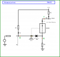
Here are two drawings. They are the same except the second has the diode replaced with a DC voltage source with the polarity shown. I'll ask a couple questions first then we can go from there if you like.
Oh and the voltage source on the far left can come in later for now it's not used at all. That will be the input signal eventually. Also note that the CCCS is the current controlled current source with gain Beta. The current sense is just a short that can sense current, and it is sensing the base current INSIDE the transistor so i labeled it 'Ibs' while the EXTERNAL base current is simply 'ib'. It doesnt make any difference in these circuits because we have to input signal yet, but it will at some point once we get into it a bit more.
Just in case you didnt notice yet, Vb is the voltage from base to ground, Vbe is the voltage from the base to emitter so they are not the same when there is an emitter resistor.
A couple questions:
1. Do you understand why the diode was replaced with a voltage source?
2. Do you think you can come up with an expression for the output voltage which here is the voltage at the collector Vc?
This expression will have to include Vcc, R1, R2, R3, and Beta which you can write as simply 'B'.
Attachments
-
 41.6 KB Views: 9
 -
 41.5 KB Views: 9
I hope i can answer only the first question, because the second is somewhat difficult. On the first question, i may give an wrong answer. Well I will have a try. The diode is placed there because it represents the voltage drop on the p-n junction of the base-emitter of the transistor. It indicates the forward biasing voltage which is equal to 0.5-0.75V. I think it is to enable the Base-emitter junction so the collector current could pass through emitter. The CCCS has the sense because i think, it allows more current to pass as the sense sense more current. That's why it is called Current controlled. The CCCS is depended on this sense in order to output the maximum current provided by Ic. At least this is what i see in the imageHello again Paul,
Here are two drawings. They are the same except the second has the diode replaced with a DC voltage source with the polarity shown. I'll ask a couple questions first then we can go from there if you like.
Oh and the voltage source on the far left can come in later for now it's not used at all. That will be the input signal eventually. Also note that the CCCS is the current controlled current source with gain Beta. The current sense is just a short that can sense current, and it is sensing the base current INSIDE the transistor so i labeled it 'Ibs' while the EXTERNAL base current is simply 'ib'. It doesnt make any difference in these circuits because we have to input signal yet, but it will at some point once we get into it a bit more.
Just in case you didnt notice yet, Vb is the voltage from base to ground, Vbe is the voltage from the base to emitter so they are not the same when there is an emitter resistor.
A couple questions:
1. Do you understand why the diode was replaced with a voltage source?
2. Do you think you can come up with an expression for the output voltage which here is the voltage at the collector Vc?
This expression will have to include Vcc, R1, R2, R3, and Beta which you can write as simply 'B'.
In the second image, if i remember well there was a formula. It's Vc=Vcc-IcRc.
Last edited:
Thanks for the encouraging words.....yet I do not resign (I am already in the eighties...)Dont feel bad you are not the only one. I've done that myself a number of times. Also, just got cataract surgery and in recovery for maybe another three weeks (ha ha).
The thing is i guess to keep pushing on and keep going. Mistakes happen but if we give up that's probably the biggest mistake.
Oh wow that's amazing! You cant be doing too bad if you still post right?Thanks for the encouraging words.....yet I do not resign (I am already in the eighties...)
I wish you many more years on top of that
Ok not badI hope i can answer only the first question, because the second is somewhat difficult. On the first question, i may give an wrong answer. Well I will have a try. The diode is placed there because it represents the voltage drop on the p-n junction of the base-emitter of the transistor. It indicates the forward biasing voltage which is equal to 0.5-0.75V. I think it is to enable the Base-emitter junction so the collector current could pass through emitter. The CCCS has the sense because i think, it allows more current to pass as the sense sense more current. That's why it is called Current controlled. The CCCS is depended on this sense in order to output the maximum current provided by Ic. At least this is what i see in the image
In the second image, if i remember well there was a formula. It's Vc=Vcc-IcRc.
This is where we get a little deeper.
Can you calculate Ic now? Because if you can, you can calculate the collector voltage.
See what you can do with that.
I think it is Ic=Vcc-(Vc/Rc). I don't know if i answered right. Otherwise it's Ic=β*IbOk not bad
This is where we get a little deeper.
Can you calculate Ic now? Because if you can, you can calculate the collector voltage.
See what you can do with that.
Ic=Vcc-(Vc/Rc)I think it is Ic=Vcc-(Vc/Rc). I don't know if i answered right. Otherwise it's Ic=β*Ib
You KNOW this is wrong because the units don't work out. Vc/Rc is a current, but you are then trying to subtract it from Vcc, which is a voltage.
Hi again,I think it is Ic=Vcc-(Vc/Rc). I don't know if i answered right. Otherwise it's Ic=β*Ib
Your second expression is correct, a very well known expression for bipolar transistors. You'll use that many times.
I like taking this slow because it gives us both time to think.
Ok so then the next step so to solve for Ib. That may be a little harder but see what you can figure out.
Just keep in mind that the base to emitter is now a voltage source which we usually set at 0.7 volts for these kinds of problems in this setting, and the base current and collector current add and that makes the emitter current the sum.
Also, only the base current flows through the diode.
See what you think and if it seems too hard dont worry it will get very easy very soon


