I need your help on CE amplifier

ericgibbs

Joined Jan 29, 2010
21,444
hi Paul,
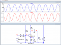
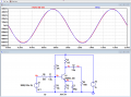
This is a suitable amplifier for your CE study, the GBW is higher than 20kHz, but should not be a problem.
Vin 40mVppk , Vout 1Vppk = Gain of 25 at 1kHz

E

Added image showing overlay of Vin and Vout.
 

Attachments

Last edited:

LvW

Joined Jun 13, 2013
2,029
Paul, perhaps some explanations to the above shown solution is helpful

* The gain of an CE-stage (Re bypassed with C) is G=-gm*Rc
* The transconductance gm is the slope of the Ic=f(Vbe) curve: gm=Ic/Vt
* Therefore: G=-Ic*Rc/Vt
* For G=25 and Vt=25mV we have: IcRc=-25*25mV=-0.625V
* That means: The DC collector potential is only 0.625V below the power rail. This is not sufficient because of distortion and clipping.
* That means: The resistor Rc (and the gain) must be increased - and, at the same time we must use an additional series resistor R6 in front of the base (voltage division) in order to bring the gain back to 25.
* That is the solution as presented in the last post#21 by Eric.
 
Last edited:

Thread Starter

PaulEngineer

Joined Dec 21, 2016
217
Very helpful solutions. With them I have almost a little bit of an idea on what happening here. But in my case, i need more better personal study. It is hard to understand all of this weird science of electronics, but at least, after a very good reading on transistor concepts, i hope i will be able to design my very own CE amplifier. Thank you everyone for the best efforts.
 

Audioguru again

Joined Oct 21, 2019
6,826
The video has the transistor audio circuit designed with as much gain and as much distortion that is possible.
It "guessed" that the beta is 200 but did not calculate if the transistor is saturated if its beta is 300 or if it is cutoff if its beta is 100.
 

dcbingaman

Joined Jun 30, 2021
1,065
Here is one way to go about it:
1 - The output impedance is determined solely by the collector resistor value. Choose what output impedance you want. Let's start with say 10K collector resistor.
2 - determine what DC bias voltage value do you want, typically you would shoot for 1/2 the supply voltage. For example, if the supply voltage is 12V then you will want to shoot for 6V. The DC bias current is then 6V/10K or 0.6mA.
3 - determine the voltage gain you want, say a gain of -10. The gain will always be negative for an CE amplifier. In order to achieve this gain you will want about 1/10 of the signal feed back to the base via negative feedback, in this case 1K is 1/10 of 10K. The voltage across the 1K would be 1/10 that of Rc voltage or around 0.6V.
4 - We now need to bias the base, in this case we need it around 0.6V plus the BE drop of 0.7V or about 1.4V. Note the input signal should not swing more than say 0.2V or you will get distortion with this setup.
5 - Determine the minimum impedance looking into the base, this would be the worst case current gain for the selected transistor multiplied by the emitter resistor. Example, if this has a worse case gain of say 100 then the impedance looking into the base would be about 100*1K or 100K.
6 - Select DC bias resistors based on the input impedance being 100K. I recommend the bias resistors be 1/10 of the input impedance of the base so in this case 10K.
7 - Select values for the voltage divider at the base to get 1.4V biasing. Say we use 22K for the top resistor then we would need around 2.9K on the bottom side. Note: This sets your input impedance.
8 - Select an appropriate input capacitor to meet the bottom of your pass band. Say it is 20Hz (12.7 rad/s). RC must then be 1/12.7 or 78ms. We already know R is 2.9K so C then is 26uF. You want a value greater than this for good passband so way we make it 100uF.
9 - Last but not least the output capacitor would simply be calculated in the same was as step 8 with the output impedance being 10K this would be 7.8uF so use say 10uF or greater.

That is all there is to it, mostly. This will give you a working amplifier with everything within the ball park.
 

Thread Starter

PaulEngineer

Joined Dec 21, 2016
217
Here is one way to go about it:
1 - The output impedance is determined solely by the collector resistor value. Choose what output impedance you want. Let's start with say 10K collector resistor.
2 - determine what DC bias voltage value do you want, typically you would shoot for 1/2 the supply voltage. For example, if the supply voltage is 12V then you will want to shoot for 6V. The DC bias current is then 6V/10K or 0.6mA.
3 - determine the voltage gain you want, say a gain of -10. The gain will always be negative for an CE amplifier. In order to achieve this gain you will want about 1/10 of the signal feed back to the base via negative feedback, in this case 1K is 1/10 of 10K. The voltage across the 1K would be 1/10 that of Rc voltage or around 0.6V.
4 - We now need to bias the base, in this case we need it around 0.6V plus the BE drop of 0.7V or about 1.4V. Note the input signal should not swing more than say 0.2V or you will get distortion with this setup.
5 - Determine the minimum impedance looking into the base, this would be the worst case current gain for the selected transistor multiplied by the emitter resistor. Example, if this has a worse case gain of say 100 then the impedance looking into the base would be about 100*1K or 100K.
6 - Select DC bias resistors based on the input impedance being 100K. I recommend the bias resistors be 1/10 of the input impedance of the base so in this case 10K.
7 - Select values for the voltage divider at the base to get 1.4V biasing. Say we use 22K for the top resistor then we would need around 2.9K on the bottom side. Note: This sets your input impedance.
8 - Select an appropriate input capacitor to meet the bottom of your pass band. Say it is 20Hz (12.7 rad/s). RC must then be 1/12.7 or 78ms. We already know R is 2.9K so C then is 26uF. You want a value greater than this for good passband so way we make it 100uF.
9 - Last but not least the output capacitor would simply be calculated in the same was as step 8 with the output impedance being 10K this would be 7.8uF so use say 10uF or greater.

That is all there is to it, mostly. This will give you a working amplifier with everything within the ball park.
I did understand everything you said. Thank you so much sir. I will follow everyone's solutions, but first I need to understand the concepts of choosing the right components. Thank you so much for this very informative lesson. Through this i have the most of an idea how to select components. That is exactly what I was searching about. One question only. How to determine what values should have R1 and R2? This is the only thing I have lost here. Thank you
 

ericgibbs

Joined Jan 29, 2010
21,444
hi Paul,
Added the Voltage and Current values at some CE amp nodes on the circuit Post #21.

You can now use these values to check your maths, if you feel like reverse engineering the circuit.
E

EG 914.png
 

dcbingaman

Joined Jun 30, 2021
1,065
I did understand everything you said. Thank you so much sir. I will follow everyone's solutions, but first I need to understand the concepts of choosing the right components. Thank you so much for this very informative lesson. Through this i have the most of an idea how to select components. That is exactly what I was searching about. One question only. How to determine what values should have R1 and R2? This is the only thing I have lost here. Thank you
R1 and R2 select the bias for the base voltage. In the example given we want to select values that will not change the DC collector voltage much from 1/2 of the supply voltage. So the ratio of R1 to R2 gives the base voltage: Vb=V*(R2/(R1+R2)). In this example that ratio needed to be about 1.4V at the base or for a 12V supply voltage around 0.12. After you find the ratio we now do not want the voltage at the base to move much when loaded by the base. One rule of thumb is 10 to 1. You want the parallel resistance of R1 and R2 to be 1/10 or less than the impedance looking into the base. Hope that helps answer your question.
 

Thread Starter

PaulEngineer

Joined Dec 21, 2016
217
R1 and R2 select the bias for the base voltage. In the example given we want to select values that will not change the DC collector voltage much from 1/2 of the supply voltage. So the ratio of R1 to R2 gives the base voltage: Vb=V*(R2/(R1+R2)). In this example that ratio needed to be about 1.4V at the base or for a 12V supply voltage around 0.12. After you find the ratio we now do not want the voltage at the base to move much when loaded by the base. One rule of thumb is 10 to 1. You want the parallel resistance of R1 and R2 to be 1/10 or less than the impedance looking into the base. Hope that helps answer your question.
That was more than helpful. Now I have everything in detail to calculate everything. Thank you so much sir. I have built a whole image on how CE amplifier works, even if it is in a basic form. Thank you for explanation on how to calculate the R1 and R2 too.
 

Audioguru again

Joined Oct 21, 2019
6,826
The current in the base bias resistors is 20 times the base current and the emitter resistor has plenty of voltage across it allowing transistors with different hFE current gain.

The circuit was designed for a transistor with a hFE of 200 but you cannot buy one with 200, some are 100 and others are 300. Will it work without causing clipping with 100 or 300 transistors?
 

ericgibbs

Joined Jan 29, 2010
21,444
hi agu,
For starters, the Base bias chain current is not 20 times greater than the Collector current..
ie: Divider 145uA , Ic = 1.4mA ,,, that on my calculator is 10 times, as it should be.

The circuit was designed so that R3 [ the input resistor ] can be adjusted to set
the Gain to 25, for various transistor Beta values, this example is for B=100

Before you say, I know that the Input impedance will lower, but this for a TS study.

I have been designing audio amps since the early 60's, no complaints so far...;)
E

Added a 2nd plot, using Beta=300., increased R3 as required.

EG 915.pngEG 916.png
 
Last edited:

Audioguru again

Joined Oct 21, 2019
6,826
Good, there is barely any change in the transistor's operation since the base bias divider has a fairly high current and the emitter resistor has a high voltage. I have never used such a high voltage on a bypassed emitter resistor.
 

MrChips

Joined Oct 2, 2009
34,820
I will repeat what dcbingaman has already written in post #26.
(My step numbers do not match his. Our procedures are practically the same.)

1) You start with the output impedance and work backwards.
Select a supply voltage and output impedance, for example Vcc = 6V and Rc = 10kΩ.

2) Set Vc to half of Vcc. Vc = Vcc / 2 = 3V

3) Now you can determine Ic = (Vcc - Vc) / Rc = 3V / 10kΩ = 0.3mA

4) Select a voltage gain, for example, Av = -10

5) Calculate RE ≅ - Rc / Av = 10kΩ / 10 = 1kΩ

6) Assume IE ≅ Ic = 0.3mA

7) Calculate voltage across RE = IE x RE = 0.3mA x 1k = 0.3V

8) Assume VB = 0.7V + VE = 1V

9) Assume current gain β= 100

10) IB = IC / β = 300μA / 100 = 3μA

11) Create a voltage divider with R1 and R2 to provide VB across R2 and 10 x IB flowing in R1 and R2.

12) Select C1 and C2 signal coupling capacitors for low frequency response.

13) Simulate and tweak R1 and R2 to suit.
 

ericgibbs

Joined Jan 29, 2010
21,444
Good, there is barely any change in the transistor's operation since the base bias divider has a fairly high current and the emitter resistor has a high voltage. I have never used such a high voltage on a bypassed emitter resistor.
hi agu,
The other advantage is that the Zout, output impedance is Low, approx 1k5.

E
 

dcbingaman

Joined Jun 30, 2021
1,065
I will repeat what dcbingaman has already written in post #26.
(My step numbers do not match his. Our procedures are practically the same.)

1) You start with the output impedance and work backwards.
Select a supply voltage and output impedance, for example Vcc = 6V and Rc = 10kΩ.

2) Set Vc to half of Vcc. Vc = Vcc / 2 = 3V

3) Now you can determine Ic = (Vcc - Vc) / Rc = 3V / 10kΩ = 0.3mA

4) Select a voltage gain, for example, Av = -10

5) Calculate RE ≅ - Rc / Av = 10kΩ / 10 = 1kΩ

6) Assume IE ≅ Ic = 0.3mA

7) Calculate voltage across RE = IE x RE = 0.3mA x 1k = 0.3V

8) Assume VB = 0.7V + VE = 1V

9) Assume current gain β= 100

10) IB = IC / β = 300μA / 100 = 3μA

11) Create a voltage divider with R1 and R2 to provide VB across R2 and 10 x IB flowing in R1 and R2.

12) Select C1 and C2 signal coupling capacitors for low frequency response.

13) Simulate and tweak R1 and R2 to suit.
I like your description better than mine. It is clearer and easier to follow. Good job describing it.
 
Top