Facebook
 Google
 GitHub
 Linkedin

What does the circuit do?
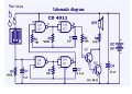
When the rain sensor is dry, IC1 pin-1 is pulled down by R1 to 0V (logic LOW).
(We call the -ve terminal of the 9V battery our COMMON voltage reference point or node. All voltage measurements are taken with respect to this common node. LOGIC LOW would be 0V. LOGIC HIGH would be Vcc or 9V).
IC1 is a quad AND gate with inverted outputs, i.e. the output is ACTIVE LOW. That is what the circle or bubble on the output signifies. We call this a NAND gate. With a LOW level at pin-1, pin-3 is HIGH and so is pin-5 and pin-6. With pins 5 and 6 tied together that NAND gate becomes a NOT gate or INVERTER. Hence pin-4 is LOW.
Similarly, pin-12 is held LOW and pin-10 is also LOW, with gate at pins 8 ,9, 10 also acting as a NOT gate.
Transistors Q1 and Q2 are in the OFF state. No current flows through SPK and R6.
The voltage at R6, Q1 and Q2 collectors would be HIGH or 9V.
IC1 constitutes two square wave oscillators.
When the sensor is wet, IC1 pin-1 is pulled up to logic HIGH. This enables the first AND gate and the circuit oscillates at a relatively low frequency determined by R2 and C2.
On the HIGH portion of the square wave cycle, pin-4 enables the AND gate at pin-12, causing that portion of the circuit to oscillate at a relatively higher frequency determined by R3 and C3.
Compare the values of R2 and C2 with R3 and C3.
As a rough guide, calculate TIME CONSTANT = R x C
1MΩ x 0.1μF = 0.1s => 10 Hz
500kΩ x 0.001μF = 0.5 x 0.001s = 0.5ms => 2kHz
Try changing the values of C2 and C3.
For example, replace C3 with 0.002μF or 0.005μF. How would this affect the tone generated by the loudspeaker?
Replace, C2 with 0.2μF and 0.5μF. How would this affect the sound produced?
When the sensor is wet the circuit oscillates. Hence voltage readings will be meaningless because the DMM is seeing rapidly changing voltages. It only makes sense to take voltage readings when the sensor is dry.
Spend more time playing and analyzing this relatively simple circuit. There is so much more that you can learn with this exercise.
When the rain sensor is dry, IC1 pin-1 is pulled down by R1 to 0V (logic LOW).
(We call the -ve terminal of the 9V battery our COMMON voltage reference point or node. All voltage measurements are taken with respect to this common node. LOGIC LOW would be 0V. LOGIC HIGH would be Vcc or 9V).
IC1 is a quad AND gate with inverted outputs, i.e. the output is ACTIVE LOW. That is what the circle or bubble on the output signifies. We call this a NAND gate. With a LOW level at pin-1, pin-3 is HIGH and so is pin-5 and pin-6. With pins 5 and 6 tied together that NAND gate becomes a NOT gate or INVERTER. Hence pin-4 is LOW.
Similarly, pin-12 is held LOW and pin-10 is also LOW, with gate at pins 8 ,9, 10 also acting as a NOT gate.
Transistors Q1 and Q2 are in the OFF state. No current flows through SPK and R6.
The voltage at R6, Q1 and Q2 collectors would be HIGH or 9V.
IC1 constitutes two square wave oscillators.
When the sensor is wet, IC1 pin-1 is pulled up to logic HIGH. This enables the first AND gate and the circuit oscillates at a relatively low frequency determined by R2 and C2.
On the HIGH portion of the square wave cycle, pin-4 enables the AND gate at pin-12, causing that portion of the circuit to oscillate at a relatively higher frequency determined by R3 and C3.
Compare the values of R2 and C2 with R3 and C3.
As a rough guide, calculate TIME CONSTANT = R x C
1MΩ x 0.1μF = 0.1s => 10 Hz
500kΩ x 0.001μF = 0.5 x 0.001s = 0.5ms => 2kHz
Try changing the values of C2 and C3.
For example, replace C3 with 0.002μF or 0.005μF. How would this affect the tone generated by the loudspeaker?
Replace, C2 with 0.2μF and 0.5μF. How would this affect the sound produced?
When the sensor is wet the circuit oscillates. Hence voltage readings will be meaningless because the DMM is seeing rapidly changing voltages. It only makes sense to take voltage readings when the sensor is dry.
Spend more time playing and analyzing this relatively simple circuit. There is so much more that you can learn with this exercise.