MisterBill2
- Joined Jan 23, 2018
- 27,741
I would not expect that 7400-series TTL devices will operate adequately in conjunction with CMOS devices.
They'll be fine at driving the TTL, although as I suspect q12x is using 74LS74's, the resistors should probably be made no larger than 2k Ohms, to satisfy the Low level input requirement. I mostly use HC or HCT versions, so I don't care!I would not expect that 7400-series TTL devices will operate adequately in conjunction with CMOS devices.
I agree with you, whether it's the older CD or the newer HC, HCT or even newer versions, CMOS rules for numerous reasons.Given that the discussion started out with CD4017's, which are about "as CMOS" as can be, I would stick with CMOS, because I prefer it, and with only one family there are fewer potential issues. And besides, CD4013 devices are so easily available.
Im always forgetting about these types and you always have to remind me about them. I will never learn.I would not expect that 7400-series TTL devices will operate adequately in conjunction with CMOS devices.
You dont have to suspect anything, you have my IC list, remember? And yes, I have 7474-74LS74 17/20.as I suspect q12x is using 74LS74's
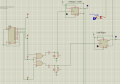
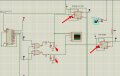
I made your 2xOR version and is still giving errors on the output.This is the pulse output version of the circuit I suggested earlier this morning!
View attachment 321586
If you don't have any OR gates, just use NOR's and put the 2 unused gates on the outputs as inverters!

- The solution is to widen this pulse signal !See my corrected version of post #40, which does switch the FF's in the correct order. However, you may have to reset the FF's with the same reset pulse that resets the 4017 each time round the loop to maintain the correct output sequence!I made your 2xOR version and is still giving errors on the output.
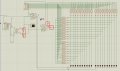
But it is switching left and right at the correct times (B_FF). It is not switching correctly the (-) rails, responsible is A_FF. And is repeating 3 times until switching (-) rails in both senses
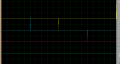
View attachment 321647
I had to tweak the osciloscope quite a lot until I got these readings and you observe the last yellow line (A_FF input) is positive and is right at the very end. The blue is for (B_FF input)
It is doing the pulse alright but I believe the FF's are not catching the pulse quite right. The same issue was with my initial pulse gen.
I think yours is better.
View attachment 321649 - The solution is to widen this pulse signal !
We need to insert a bit of delay in this pulse mechanism. Hmmm...
My modified circuit certainly works, because I tested it, and it gives the outputs you require.another try
the tests were promising but when put into my cct, failed. Couldn't clock anything.
View attachment 321661
Here is the effect:My modified circuit certainly works, because I tested it, and it gives the outputs you require.


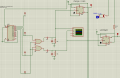
Forget what I said about the amended circuit in post #40, it doesn't work in practice, and is indeed far too complex. ALL that is needed in fact is to connect Pin 2 "1", and Pin 7 "3", to one OR gate, connected via the cap and resistor/diode arrangement to FF "A". Then just connect Pin 4 "2" to the other gate (both inputs commoned, as a driver), then via the capacitor, etc, as before, to FF "B". That DOES work, I have it running on my bench now!Hmmm, I believe I find the problem. You see that blue btn in green square. He is 0 all the time, 1 when is pressed and then returns to 0 when I release it.
When I did the tests, I used that type of button. Now, in the cct, those CLK pins are staying High for some reason. We need to keep them Low all the time, and when the pulse is activated, will go 0-1-0 and remain on 0 even after 4017 clocked next.
View attachment 321668
-
Ok, I changed those 2 10k into 1k and both CLK pins are staying Low all the time.
But the output is still erroneous.
-
Ive added 1k to the AND gates, maybe was too much current surge. I THINK... but not sure, it influenced it a bit/changed the behaviour a bit maybe?
This is a movie, not a picture, see -link-
You can see is starting ok but after some passes, is going in error land.
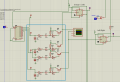
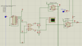
Those red marks are the recent changes + overall look of the cct.
View attachment 321667
Like this?Forget what I said about the amended circuit in post #40, it doesn't work in practice, and is indeed far too complex. ALL that is needed in fact is to connect Pin 2 "1", and Pin 7 "3", to one OR gate, connected via the cap and resistor/diode arrangement to FF "A". Then just connect Pin 4 "2" to the other gate (both inputs commoned, as a driver), then via the capacitor, etc, as before, to FF "B". That DOES work, I have it running on my bench now!
It does need the reset from the 4017 connected to the FF resets via an inverter if using 74LS74's. This wouldn't be the case if using a CD4013 though.

You haven't added the Reset circuitry that I used with my circuit. It's essential, otherwise the FF 's can get out of sync and flip to the wrong states.
And Congratulations ! Thank you ! Now is working !You haven't added the Reset circuitry that I used with my circuit. It's essential, otherwise the FF 's can get out of sync and flip to the wrong states.
Just connect both FF Reset pins (Pin 1's) together and connect them to the output of an inverter. Connect the inverter input to the Reset pin on the 4017.

-Did you build it on your breadboard?That DOES work, I have it running on my bench now!
Yes, I did build it, and I have it clocking away quite happily now!-Did you build it on your breadboard?
-Also do explain to me the logic you folowed and the logic that is now when is working. I do understand something but Im not completly sure I understand it fully.
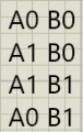
Yes, you basically explained this:The only FF which has to change twice during the cycle is "A", so starting with L L, the "1" pulse flips FF "A", and we get "B"=L. A"=H.
Next, the "2" pulse flips FF "B" and we get "B"=H, "A"=H.
Thirdly, the "3" pulse again flips FF "A" back to Low, and we get "B"=H, "A"=L
And finally, the "4" pulse resets everything and starts the cycle over!

instead of this:

If you continue successive logic sequences around the loop, without the resetting of the FF's, it becomes apparent that the next sequence becomes:Yes, you basically explained this:
View attachment 321754
-But my question was how did you think to add FF's Reset pins to the 4017 MR ? Because I didnt see it in a million years.
-And how did you think to add the OR gates? Pretty genius.
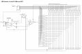
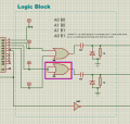
I simplified the cct a bit by removing one OR gate that was doing nothing.
I tested it and is working ok like this:
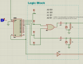
View attachment 321755instead of this:View attachment 321757
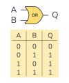
Pretty smart for the OR gate usage when the inputs are 0. Practically holding the FF CLK to 0 all the time, until 4017 changes its outputs.
Probably you chased a gate that hold its 0 inputs to a 0 output, and thats how you decided on OR gate to use.
View attachment 321756
| Thread starter | Similar threads | Forum | Replies | Date |
|---|---|---|---|---|
|
|
Looking for a schematic of a led chaser circuit. | General Electronics Chat | 49 | |
| B | Sequential LED Turn Signals | PCB Layout , EDA & Simulations | 55 | |
|
|
An LED Chaser based on a 555 and 4017. | Digital Design | 127 | |
|
|
4017 chaser leds | General Electronics Chat | 4 | |
| L | Audio Modulated 4017 Chaser | General Electronics Chat | 3 |