How does the NCP81080 dual gate driver work?
Now I’ve a circuit need used this components but I couldn’t understand it’s operation principal,
Here is datasheet
https://www.onsemi.cn/PowerSolutions/document/NCP81080-D.PDF
It’s means I need two signal HI and LI input
So if I generate square wave duty 50% one of positive another is negative for input.
So I need to delay my signal?
Because in typical timing diagram has fixture 135ns dead time
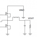
Another questions is typical application circuit output has resistor and capacitor what it’s means ?
Means one is DC loading on resistor another is AC loading on capacitor? Or RC parallel filter?
Thanks for your help...I study of this circuit several days, but still couldn’t realize this function....

 Facebook
 Google
 GitHub
 Linkedin


