How Do You Choose Decoupling Capacitors for a Microcontroller Circuit?

Thread Starter

cedricuk

Joined Sep 7, 2026
32
I’m interested in how people choose decoupling capacitors when designing microcontroller circuits.

I understand that a small capacitor placed close to the power pins helps reduce supply noise and handle sudden changes in current. However, I’m curious how you decide on the capacitance value and whether additional capacitors are needed.

Is a 100 nF ceramic capacitor a good starting point for most digital ICs, and when would you add a larger capacitor nearby? How much do capacitor placement and PCB layout affect the results?

I’d appreciate any practical advice on choosing suitable values and avoiding common mistakes.
 

nsaspook

Joined Aug 27, 2009
16,503

MrChips

Joined Oct 2, 2009
35,268
I’m interested in how people choose decoupling capacitors when designing microcontroller circuits.
The requirements for decoupling capacitors in digital circuits are different from those for analog circuits and mixed signal applications.

100 nF ceramic capacitors is standard for digital and MCU (microcontroller unit) circuits. The general guideline is one 100 nF for every IC package.

Board placement and length of capacitor leads is much more important than the actual capacitance value. This is because PCB trace and capacitor lead have series resistance and inductance which degrade the effectiveness of the capacitor to act as a high frequency filter.

Therefore, embrace SMT (surface mount technology) in your board design. Use leadless chip capacitors. Make power and ground traces wider than what you would for signal traces, at least 1 mm (0.040") or wider. Place the decoupling capacitor as close as possible to the IC power and ground pins. For more stringent requirements, on a 2-layer PCB, you would put a ground plane on the lower layer. Hence the decoupling capacitor is no more than one via away from ground.

Depending on the size, complexity, and power requirements of the board, place 10 to 100 μF electrolytic capacitor where DC power enters the board.
 

crutschow

Joined Mar 14, 2008
38,909
Added suggestion:
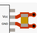
For maximum capacitor effectiveness with surface mount capacitors, run the power and ground traces into one side of the capacitor pads, and the traces to the IC out the other side of the pads (example below).
That way the trace inductance to the capacitor is kept to a minimum.

If possible, the ground side of the capacitor should go directly to a ground plane as MrChips suggested.

1792169136926.png
 
Last edited:

Thread Starter

cedricuk

Joined Sep 7, 2026
32
https://www.ti.com/content/dam/vide...mp4/subassets/notes-decoupling_capacitors.pdf

This is good place to get started. Above 50Mhz placement and ground start to get critical.

https://www.analog.com/media/en/training-seminars/tutorials/MT-101.pdf

It's both simple in theory and at times complex in applications where placement and spacing dictate compromise from the ideal on a simple PCB.
Thanks for sharing these resources. The point about placement and ground connections becoming more critical at higher frequencies is helpful. It’s interesting how a simple concept like decoupling can become more complicated when PCB layout and practical constraints come into play. I’ll take a look at the references.
 

Thread Starter

cedricuk

Joined Sep 7, 2026
32
The requirements for decoupling capacitors in digital circuits are different from those for analog circuits and mixed signal applications.

100 nF ceramic capacitors is standard for digital and MCU (microcontroller unit) circuits. The general guideline is one 100 nF for every IC package.

Board placement and length of capacitor leads is much more important than the actual capacitance value. This is because PCB trace and capacitor lead have series resistance and inductance which degrade the effectiveness of the capacitor to act as a high frequency filter.

Therefore, embrace SMT (surface mount technology) in your board design. Use leadless chip capacitors. Make power and ground traces wider than what you would for signal traces, at least 1 mm (0.040") or wider. Place the decoupling capacitor as close as possible to the IC power and ground pins. For more stringent requirements, on a 2-layer PCB, you would put a ground plane on the lower layer. Hence the decoupling capacitor is no more than one via away from ground.

Depending on the size, complexity, and power requirements of the board, place 10 to 100 μF electrolytic capacitor where DC power enters the board.
Thanks for the clear explanation. It’s helpful to understand why capacitor placement and parasitic inductance can matter more than simply increasing the capacitance value. The distinction between local 100 nF decoupling and a larger capacitor at the board’s power entry also makes sense. Appreciate the practical guidance.
 

Thread Starter

cedricuk

Joined Sep 7, 2026
32
Added suggestion:
For maximum capacitor effectiveness with surface mount capacitors, run the power and ground traces into one side of the capacitor pads, and the traces to the IC out the other side of the pads (example below).
That way the trace inductance to the capacitor is kept to a minimum.

If possible, the ground side of the capacitor should go directly to a ground plane as MrChips suggested.

View attachment 372333
Thanks for adding this detail. The explanation of routing the traces through opposite sides of the capacitor pads makes the layout advice easier to visualise. Keeping the connections short and providing a direct path to the ground plane seems especially important for effective high-frequency decoupling.
 
Top