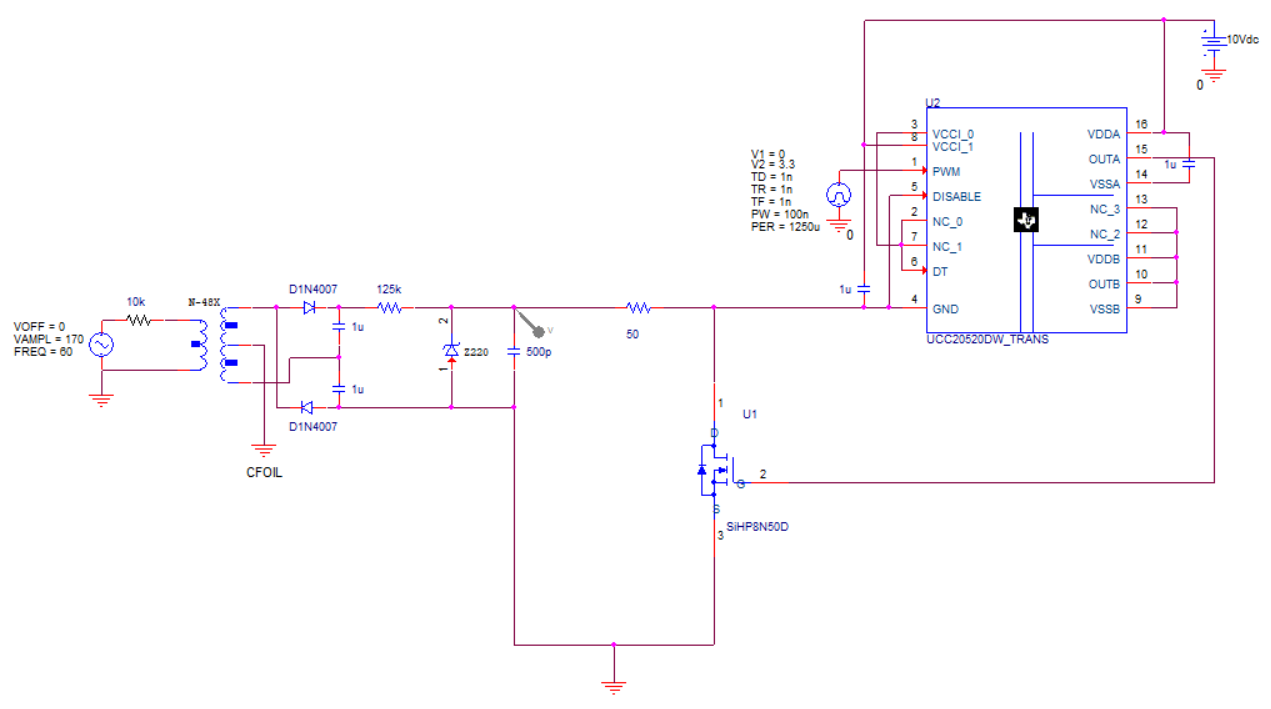
How are Power Mosfets driven by Gate Drivers if the Vgs needs to be so high?

Thread Starter

mbferguson

Joined Apr 23, 2017
94
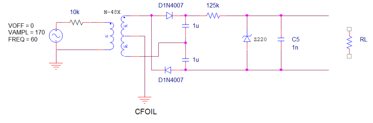
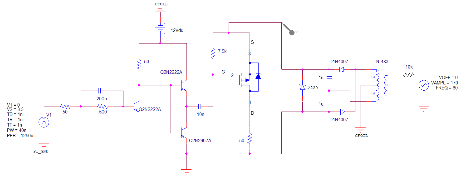
I had the basic circuit from a previous design.
Not likely, since you need a very low impedance (high current) source to rapidly switch the high capacitance of the MOSFET gate.
Is that because P-type generally have higher Rds(on) than N-type mosfets? My target is 100ns, but I realize delay times can prevent me from getting exact.

I was having trouble understanding the difference between the Qg and Vgs parameters of the power mosfets earlier. If Vgs is what 'activates' the gate and lets current flow from D->S or S->D, Qg doesn't seem like it matters too much. Although I'm sure the Vgs is charging Qg, which activates the gate... which ... magic.
 

crutschow

Joined Mar 14, 2008
38,703
Is that because P-type generally have higher Rds(on) than N-type mosfets?
Partially.
But N-types also have a significant gate capacitance.
I was having trouble understanding the difference between the Qg and Vgs parameters of the power mosfets earlier.
They are two unrelated parameters.

Vgs(th) is the gate-source voltage that just starts to turn on the MOSFET (not fully turn it on)

Qg is the gate charge (from capacitance) that must be added and removed from the gate to turn it on and off.
It's the generally high value of Qg in power MOSFETS that makes it difficult to rapidly switch a MOSFET.
So, to minimize the gate drive requirements for rapid switching, you want to look for a MOSFET with a low Qg.
 
Last edited:

Thread Starter

mbferguson

Joined Apr 23, 2017
94
Partially.
I had originally planned to use a capacitor to discharge to RL when the gate was closed like this:


The advantage of the capacitor is that it limits how much current is actually sent to the RL. I tried coming up with ways how to attach the above circuit to your example, but the best I could do was simply omitting the capacitor.


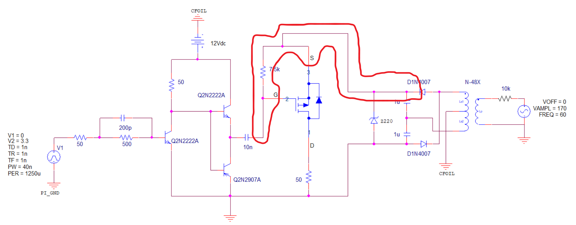
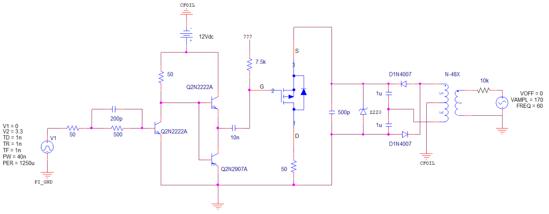
Is there a simple way to keep the capacitor without breaking the way the red labeled node works?


There doesn't seem to be any easy way to fix the '???' node.


The reason I'm concerned about sending a pure DC current is that it may deliver too much power to RL in terms of Watt. The capacitor with a discharge resistance of only ~50 ohms would quickly lose all of its current but still send the desired pulse width and amplitude. Since my sample rate is sufficiently low, the capacitor would have plenty of time to fully charge before the next cycle. I spent a few hours on Mouser playing with the parallel resistor equations trying to come up with a combination of resistors that could both: 1) Handle the DC source wattage and 2) Keep the PW near 100ns. I eventually said fudge it and decided I'd rather the load explode than buy some expensive resistors.
 

ebp

Joined Feb 8, 2018
2,332
I'll wander back later with some more details, but for now:

Your capacitor charging source is "floating" with respect to the rest of the circuit, so you have freedom to define any point, or no point, in the charging source as "ground."

You can connect your FET in common-source with the source at "signal ground" for the rest of the circuit, which means you require only a low-side driver and can use an N-channel FET.

A negative pulse is as good as a positive when it comes to pinging the probe.
 

Thread Starter

mbferguson

Joined Apr 23, 2017
94
It's unlikely there's enough energy in a 100ns pulse to damage your device.
Yes, I subconciously thought that briefly if I remember that correctly. But I am by nature paranoid of the flaws. The flawwws. Failure is not an option. :cool:
 
Last edited:

Thread Starter

mbferguson

Joined Apr 23, 2017
94
I'll wander back later with some more details, but for now:

Your capacitor charging source is "floating" with respect to the rest of the circuit, so you have freedom to define any point, or no point, in the charging source as "ground."

You can connect your FET in common-source with the source at "signal ground" for the rest of the circuit, which means you require only a low-side driver and can use an N-channel FET.

A negative pulse is as good as a positive when it comes to pinging the probe.
My mind is jello at this point. Cadence has warped me into a monster I have never imagined possible. I'll be damned if they didn't make those manufacturer spice models as hard as possible to use.

I thought there was a problem with low-side configuration because I couldn't get the cadence simulation to work correctly.

Just got finished wiring this sucker up.


*Error - "Sorry you got too many nodes. Please buy the non-student version for $1000" ༼ʘ̚ل͜ʘ̚༽
And ofcourse they didn't tell me that until I got the circuit to compile
 
Last edited:

ebp

Joined Feb 8, 2018
2,332
I don't have schematic tools on this computer, so a description;

"ground" here means the common for both transmit & receive probes, microcontroller, etc.
Shield side of transmit side of probe to ground
N-channel FET source to ground
Capacitor between drain of FET and the free side of the transmit probe
Positive from the power supply to the drain side of the cap
Negative from the power supply to probe side of the cap
NO OTHER CONNECTION from the power supply to any point in the circuit
Ordinary low-side gate driver between FET gate and ground

cap charges from "floating" power supply, discharges through probe & FET, driving probe negative with respect to signal ground

My only concern in this is that the intrinsic body diode in the FET may limit the positive going "ringing" of the probe crystal after the big negative spike. This could be solved with a diode (cathode to drain) between the FET and the probe. Believe it or not, an ordinary 1N4148 diode is likely adequate (I've bashed ultrasonic pulser energy through 1N4148s where the probe current would be in the range of 7 to 9 amperes). There are better diodes, but only in surface mount as far as I know.

There may be some merit in putting a moderate resistor, eg 1k, between each side of the capacitor and the zener, the intent being to somewhat "decouple" the capacitor and the zener from each other.


This is the doubler circuit. Note that there is no centre tap on the secondary.
upload_2018-11-25_17-39-58.gif
source: https://www.electronics-tutorials.ws/blog/voltage-multiplier-circuit.html
 
Top