
Hi People
Thank you and Have a Nice Day
Attachments
-
1.5 KB Views: 6


Hi sir, I hope you remember me. Your answer to adding the dead time between complementary PWM signal using NAND schmitt trigger logic gate can be used to drive these mosfets with dead time right?You are getting conduction through both MOSFETs being on during the switching interval.
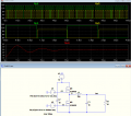
Below is the circuit with non-overlap delays added to the two switching waveforms.
See how the M2 gate signal (yellow trace) doesn't go high until after the M1 gate signal (green trace) has gone low, and goes low before the M1 gate signal goes back high.
Note that the gate voltage needs to be 5V or 10V above the supply voltage, depending upon whether the MOSFET is a logic-level, or standard type, to fully turn on the MOSFET.
In a real circuit you could do that with a bootstrap MOSFET driver circuit.
With that, the efficiency is about 88% (load power divided by V3 power).
The output has a large overshoot due to the resonance caused by the output inductor and capacitor.
The is minimized is an actual circuit by using a slow start circuit.
(I didn't have your MOSFET model so I used one I had.)
View attachment 254296
Beg to differ.Simulators are...nah..just too far out from reality.
Certainly poor models and not adequately modeling ALL parasitic elements will lead to incorrect results. Bob Pease, far more experienced in circuit models than most folks, had a great deal to say about that.Beg to differ.
I designed and simulated a low-noise, buck regulator for a NASA satellite application.
The design would have been much more difficult if not for the simulations helping me tweak the design to get the desired performance.
And the results with the actual circuit were very close to the simulated results, including noise and efficiency.
If a simulator does not give accurate results it's often the result of poor component models and/or not properly including parasitics.
Certainly true! A variable duty cycle inverter is far more forgiving than the typical switching mode supply. And the circuit shown can probably be very simply adjusted to serve as a typical 19 volt, 90 watt supply for a laptop computer for application in a vehicle. So thanks for publishing it. I am not sure just how clean the power for a typical laptop computer needs to beMake Your life easier .......
Use a "Push-Pull" Transformer Output.
Very low-Noise, Very stable, even if You don't know what you're doing.
.
.
.
View attachment 254766
True.Bob Pease, far more experienced in circuit models than most folks, had a great deal to say about that.
Of course.Knowing every element that must be included in a model is not what I would anticipate from a beginner or even most casual users of simulators. The pain is most often found in the details.

Certainly.It was NEVER a substitute for the breadboard or the bench.
This brings up an interesting point. When I was a young engineer the cost of producing a PCB was quite large in relative terms (about 1/3rd of my yearly gross income) and required the dedicated labor of numerous professionals. This was ca. 1970. Now the cost of producing a PCB, is in relative terms, a fraction of the cost that it would have taken then, due to schematic capture, PCB layout software, and automated PCB fabrication. This means that today's breadboard could actually be the 1st PCB turn as @crutschow has indicated. In those bygone days, multiple PCB turns, despite the expense, was a common occurrence.Certainly.
A simulation is part of the design process, not to generate a final production design without breadboarding.
An exception was the low noise buck regulator I designed at work, which was so layout critical that my breadboard was the first PCB after the simulations and design.
I only had to make a few slight mods for the final PCB design.
