Facebook
 Google
 GitHub
 Linkedin
Dear All,
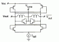
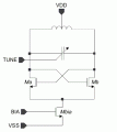
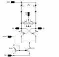
I have attached the three diagram of VCO .No.1 is VCO for NMOS only tailed bias VCO. No2 is differetial VCO . No3. is Oscillator from cross couple inverter.
Question: why they use 4 terminal NMOS as varactor ??what is the advantage of this .?
Question :In No.3 , I know the top PMOS is cross coupled and what is the function of NMOS below. It look like MEMORY circuit DRAM .Why he choose that layout and advantage?
Thanks..
Attachments
-
 5.5 KB Views: 33
 -
 4.8 KB Views: 24
 -
 2.7 KB Views: 24