Facebook
 Google
 GitHub
 Linkedin

Hi, thank you for your helpNo.
It may work in the simulation but it won't work in a real circuit.
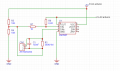
The (+) input of U2 needs a DC path for its bias current as MrChips stated.
Do you not believe that?
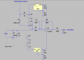
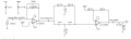
To minimize the output offset, you can provide a U2 DC gain of one by connecting a capacitor (Cx) of appropriate size for the lowest AC signal frequency, in series with R6 to ground.
Then the DC gain for offset will be 1 but the AC gain above the R6Cx rolloff is 161.
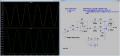
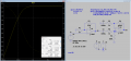
Your plots are useless to us without knowing where those signals are coming from.
Give the nodes a label (Label Net) on the schematic (e.g. In, Out, etc.) so we can tell.
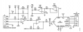
this is the whole circuit; I've added a capacitor in series with R6 at ground as you said, but in the result the 2nd OpAmp won't work anymore (the final signal is equal to the signal produced by the first OpAmp, while i need the last signal to have wave of amplitude around 6V or something like it).
can you maybe send a drawing of what should i do? thanks