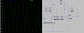
Hmmm, do you have details of this piezo device? All the ones I've used generate a voltage proportional to the stress experienced by the crystal. When we talk about electrical charge, in Coulombs, we usually mean the product of current and time ie Q = i . t, or the charge stored in a capacitor, the product of the capacitance and voltage, Q = V . C
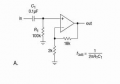
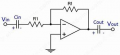
In this context I suspect 'charge' means the time-integrated output of the piezo device (voltage) across a known load resistor, e.g. ∫V(t)/R . dt which is a measure of Impulse (J = F . dt ), hence the integrator component shown.
Hmmm, do you have details of this piezo device? All the ones I've used generate a voltage proportional to the stress experienced by the crystal. When we talk about electrical charge, in Coulombs, we usually mean the product of current and time ie Q = i . t, or the charge stored in a capacitor, the product of the capacitance and voltage, Q = V . C
In this context I suspect 'charge' means the time-integrated output of the piezo device (voltage) across a known load resistor, e.g. ∫V(t)/R . dt which is a measure of Impulse (J = F . dt ), hence the integrator component shown.
The piezoelectric material used is PVDF piezofilm.
So, as we discussed, by connecting the piezo to this circuit, it should operate independently, without the use of a sort of "charge to voltage". Is that correct?
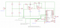
so i adjust the F for C1 and C2, if I reduce the resistance I have to put another stage in between and it will cost more, Idk, the simulation on LTSpice works, what may be the problem that occurs if I leave it like that?
what do you mean by AC coupling between stage? could you maybe send a drawing? thanks.
the piezo will work like I have done it? and so the ADS?
thank you very much!
by my calculations on the piezo, the maximum value of V generated by 300kg is 0,0000024V (g33 is 0,2 v*m/N and i have a piezo of 5cmx5cm with a height of 30micron under compression load (300kg->3000N)). so with this V, after the OpAmp i got a maximum of 3,6V
No.
It may work in the simulation but it won't work in a real circuit.
The (+) input of U2 needs a DC path for its bias current as MrChips stated.
Do you not believe that?
To minimize the output offset, you can provide a U2 DC gain of one by connecting a capacitor (Cx) of appropriate size for the lowest AC signal frequency, in series with R6 to ground.
Then the DC gain for offset will be 1 but the AC gain above the R6Cx rolloff is 161.
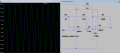
Your plots are useless to us without knowing where those signals are coming from.
Give the nodes a label (Label Net) on the schematic (e.g. In, Out, etc.) so we can tell.
by my calculations on the piezo, the maximum value of V generated by 300kg is 0,0000024V (g33 is 0,2 v*m/N and i have a piezo of 5cmx5cm with a height of 30micron under compression load (300kg->3000N)). so with this V, after the OpAmp i got a maximum of 3,6V

 Facebook
 Google
 GitHub
 Linkedin