Full bridge inverter with charger

Ian0

Joined Aug 7, 2020
13,158
I still see issues with the seven volt winding. I am missing how seven volts into an "H bridge" is going to charge a 12 volt battery, which requires a least 14 volts.
You're missing that the H-bridge operates as a synchronous buck regulator when it is an inverter and as a synchronouis boost regulator when it is a charger.
 

Thread Starter

Joeadeoye

Joined Apr 2, 2017
49
Thi
I still see issues with the seven volt winding. I am missing how seven volts into an "H bridge" is going to charge a 12 volt battery, which requires a least 14 volts.
This is exactly the problem I am trying to solve. As 7v is too small to charge a 12v battery
 

MisterBill2

Joined Jan 23, 2018
27,720
Thi
This is exactly the problem I am trying to solve. As 7v is too small to charge a 12v battery
The challenge is that for most switching mode converters there has to be an inductance to store the energy so that it can be delivered at a different voltage level.
So that is why I suggested a full-wave voltage doubler in posts #2 and #6. And I suggested using separate diodes because I am not sure how to implement it using the "H" bridge circuit of the inverter.
It would be doubling the peak voltage at the point of rectifying, so the same transformer could easily be used. In addition, since it would be a separate circuit from the inverter, there would not need to be any compromises in components or circuits. THAT would make the design a much simpler task.
There might even be a scheme to do it with the diodes in the mosfets,
 

MisterBill2

Joined Jan 23, 2018
27,720
I am having a difficult time visualizing how that would be arranged, given that in most switchers there is circuit both ahead and behind the energy storage inductance. Could you provide a circuit showing how that would work??
 

Ian0

Joined Aug 7, 2020
13,158
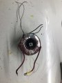
I’ll draw a diagram when I’m back at home. Here’s a photo of the type of transformer used in a Victron inverter/charger.8553765D-EA3D-4255-8031-A0686412BE54.jpeg
You can see that the low-voltage winding covers only about half the core, which gives a leakage inductance of 22mH Referred to the high-voltage winding.
 

Ian0

Joined Aug 7, 2020
13,158
Screenshot from 2024-06-12 18-37-26.png
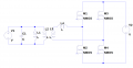
V1 is the mains (its source resistance and inductance are not shown)
V2 is the battery.
C1 is the filter capacitor from when it works as an inverter
L1 is the magnetising inductance of the transformer
L2 and L3 are the transformer
L4 is the transformer's leakage inductance.
Compared to the PWM frequency the voltage at L3dot can be assumed to be DC, and is of lower magnitude than the battery voltage.
In the half-cycle where the dot is positive, M4 is switched on throughout the half-cycle
M2 switches on, which looks like a dead-short on the transformer, except for the large leakage inductance L4.
Current increases in L4.
M2 switches off and M1 switches on.
L4 current then flows into the battery.
PWM cycle repeats.
In the half cycle where the dot is negative M2 is switched on throughout the half-cycle
M4 switches on and current builds up in L4.
M4 switches off and M3 switches on and current flows in to the battery.

It is essentially the same operation as a bridgeless PFC circuit (where "bridgeless" means there is no diode bridge)
 

Thread Starter

Joeadeoye

Joined Apr 2, 2017
49
The challenge is that for most switching mode converters there has to be an inductance to store the energy so that it can be delivered at a different voltage level.
So that is why I suggested a full-wave voltage doubler in posts #2 and #6. And I suggested using separate diodes because I am not sure how to implement it using the "H" bridge circuit of the inverter.
It would be doubling the peak voltage at the point of rectifying, so the same transformer could easily be used. In addition, since it would be a separate circuit from the inverter, there would not need to be any compromises in components or circuits. THAT would make the design a much simpler task.
There might even be a scheme to do it with the diodes in the mosfets,
Pls can you share the full bridge voltage doubler circuit you're talking about?
 

Thread Starter

Joeadeoye

Joined Apr 2, 2017
49
T
View attachment 324463
V1 is the mains (its source resistance and inductance are not shown)
V2 is the battery.
C1 is the filter capacitor from when it works as an inverter
L1 is the magnetising inductance of the transformer
L2 and L3 are the transformer
L4 is the transformer's leakage inductance.
Compared to the PWM frequency the voltage at L3dot can be assumed to be DC, and is of lower magnitude than the battery voltage.
In the half-cycle where the dot is positive, M4 is switched on throughout the half-cycle
M2 switches on, which looks like a dead-short on the transformer, except for the large leakage inductance L4.
Current increases in L4.
M2 switches off and M1 switches on.
L4 current then flows into the battery.
PWM cycle repeats.
In the half cycle where the dot is negative M2 is switched on throughout the half-cycle
M4 switches on and current builds up in L4.
M4 switches off and M3 switches on and current flows in to the battery.

It is essentially the same operation as a bridgeless PFC circuit (where "bridgeless" means there is no diode bridge)
This looks interesting, but I'm having hard time understanding it.
 

MisterBill2

Joined Jan 23, 2018
27,720
It IS NOT a "full bridge" doubler, but it is a FULL WAVE voltage doubler. Really, it is two half wave rectifiers stacked on each other.
Now I am really wondering how an "engineer" who was able to make an inverter as complex as we see in post #1, and have it working, is not aware of a voltage doubler circuit.
So here is the detailed description: on one side there are two diodes in series, both pointing UP. On the other side are two polasrized electrolytic capacitors in series, with the positive side up. The top of the upper capacitor is connected to the top of the upper diode, the negative of the lower capacitor is connected to the bottom of the lower diode. That junction is the negative end of the doubler. The top junction is the positive end of the doubler. The AC input is between the connection between the two capacitors and the connection between the two diodes.
During an AC cycle, when the junction of the two capacitors is positive, the lower capacitor is charged by the positive voltage. when the connection between the two diodes is positive, the top capacitor is charged. so the voltage between the top and the bottom is twice the peak AC input voltage.
I hope that all were able to draw the circuit from my description. It is a classic, often presented in the last weeks of the second semester of basic electrical circuits classes.
 

Thread Starter

Joeadeoye

Joined Apr 2, 2017
49
It IS NOT a "full bridge" doubler, but it is a FULL WAVE voltage doubler. Really, it is two half wave rectifiers stacked on each other.
Now I am really wondering how an "engineer" who was able to make an inverter as complex as we see in post #1, and have it working, is not aware of a voltage doubler circuit.
So here is the detailed description: on one side there are two diodes in series, both pointing UP. On the other side are two polasrized electrolytic capacitors in series, with the positive side up. The top of the upper capacitor is connected to the top of the upper diode, the negative of the lower capacitor is connected to the bottom of the lower diode. That junction is the negative end of the doubler. The top junction is the positive end of the doubler. The AC input is between the connection between the two capacitors and the connection between the two diodes.
During an AC cycle, when the junction of the two capacitors is positive, the lower capacitor is charged by the positive voltage. when the connection between the two diodes is positive, the top capacitor is charged. so the voltage between the top and the bottom is twice the peak AC input voltage.
I hope that all were able to draw the circuit from my description. It is a classic, often presented in the last weeks of the second semester of basic electrical circuits classes.
I understand your explanation perfectly, if i'm not mistaking, your explanation is same as the circuit posted by Dodgydave in #4 comment. I know it will double the voltage, but my question is, can it give enough current to charge a 220AH battery, without experiencing voltage drop? Let's say for example, the voltage doubler circuit outputs 14v from 7v input. Can it deliver upto 10A current while maintaining the 14v
 

MisterBill2

Joined Jan 23, 2018
27,720
In a voltage doubled it is the capacitors that limit the available current, Unfortunately the regulation is not good, so some calculations will be required to determine the needed capacitance.
 

Thread Starter

Joeadeoye

Joined Apr 2, 2017
49
In a voltage doubled it is the capacitors that limit the available current, Unfortunately the regulation is not good, so some calculations will be required to determine the needed capacitance.
"it is the capacitors that limit the available current" this is exactly what i have been thinking and i haven't been able to figure out the amount of capacitance that will be sufficient to deliver 10Amps, or even 20Amps. The amount of capacitance will be out of the box...
 

Thread Starter

Joeadeoye

Joined Apr 2, 2017
49
View attachment 324463
V1 is the mains (its source resistance and inductance are not shown)
V2 is the battery.
C1 is the filter capacitor from when it works as an inverter
L1 is the magnetising inductance of the transformer
L2 and L3 are the transformer
L4 is the transformer's leakage inductance.
Compared to the PWM frequency the voltage at L3dot can be assumed to be DC, and is of lower magnitude than the battery voltage.
In the half-cycle where the dot is positive, M4 is switched on throughout the half-cycle
M2 switches on, which looks like a dead-short on the transformer, except for the large leakage inductance L4.
Current increases in L4.
M2 switches off and M1 switches on.
L4 current then flows into the battery.
PWM cycle repeats.
In the half cycle where the dot is negative M2 is switched on throughout the half-cycle
M4 switches on and current builds up in L4.
M4 switches off and M3 switches on and current flows in to the battery.

It is essentially the same operation as a bridgeless PFC circuit (where "bridgeless" means there is no diode bridge)

I have read this over and over again, what i want to understand is the switching of the 4 mosfets. From what i can grasp so far, this is going to have 4 modes of current flow throughout one cycle. Lets assume we are switching at 50Hz (frequency), then one complete cycle will cover 20ms (time), which means positive cycle is 10ms and negative cycle is 10ms respectively.

Mode 1:
In the half-cycle where the dot is positive, M4 is switched on throughout the half-cycle: M4 is ON for 10ms
M2 switches on, which looks like a dead-short on the transformer, except for the large leakage inductance L4.: M2 is ON for 5ms thus allows current to flow into L4 (Current increases in L4.)

Mode 2:
M2 switches off and M1 switches on.: M2 turns OFF after 5ms and M1 turns ON for the remaining 5ms (keep in mind that M4 is still ON) thus allowing current from both L4 and transformer itself to flow to the battery (V2) through M1 and return path M4
L4 current then flows into the battery.

Mode 3:
In the half cycle where the dot is negative M2 is switched on throughout the half-cycle: M2 is ON for 10ms
M4 switches on and current builds up in L4.: M4 turns ON for 5ms and allows current to build up in L4

Mode 4:
M4 switches off and M3 switches on and current flows in to the battery: M4 turns OFF after 5ms and M3 turns ON for the remaining 5ms (keep in mind that M2 is still ON), allowing current to flow from L4 through M3 to the battery (V2) and return path M2

This completes the operation in one cycle (20ms, assuming we are switching at 50Hz). I want to be sure i get your explanation right before i proceed. Am i correct?
 

Ian0

Joined Aug 7, 2020
13,158
I am still having trouble thinking that the leakage inductance will function as a useful inductor for energy storage.
Is it any different from adding a real, physical inductor in series with the winding of a “perfect” transformer? (Or as close to perfect as one can get). Think of all those leakage reactance transformers that were used for neon lamps, or indeed for current limiting in primitive battery chargers.
You could even think about ferroresonant transformers. . . . .
 

MisterBill2

Joined Jan 23, 2018
27,720
It may indeed be different, that is what the hang-up is.
Note that I am not trying to argue about it, just having a hard time with it.
Certainly the majority of UPS devices have only one large transformer, and most of them only have that single mains frequency transformer, any other is much smaller and made for a much higher frequency. And I have not come across an actual detailed circuit of a respectable commercialy available UPS. But I have observed that many of them include quite a few relays with medium heavy-current contacts. So there is some circuit change happening between charge and operate modes. And they would not go to that expense if it were not needed.
 

Ian0

Joined Aug 7, 2020
13,158
It may indeed be different, that is what the hang-up is.
Note that I am not trying to argue about it, just having a hard time with it.
Certainly the majority of UPS devices have only one large transformer, and most of them only have that single mains frequency transformer, any other is much smaller and made for a much higher frequency. And I have not come across an actual detailed circuit of a respectable commercialy available UPS. But I have observed that many of them include quite a few relays with medium heavy-current contacts. So there is some circuit change happening between charge and operate modes. And they would not go to that expense if it were not needed.
The big relays would do the following:
  • Disconnect the input from the transformer when it is inverting (otherwise it feeds back into the mains)
  • Connect the outgoing neutral to earth.
 
Top