Facebook
 Google
 GitHub
 Linkedin
hello! i am a second year first semester EENG student, and for the digital project this semester we are tasked with programming a fpga to do something (i.e. clock, calculator, stop light, etc).
Disclaimer:
*the project requirements does not include creating a circuit. most/all are simply using the on-board IO on the basys3 development board.
*i am not asking for code, only schematic/ pcb help.
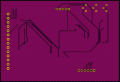
for my project i want to create something like this:
below is my schematic, but first i will describe it to the best of my ability. i want for the motor (12vdc) to spin at a speed set either by the on-board potentiometer or via SPI, whenever a switch is triggered (if you watch the video, the switch is on the arm), for a set amount of time. this will control a total of three spool holders (systems of 1x POT, 1x Switch, 1x Motor, 2x LED). led EN shows whether or not the POT is enabled or is under SPI control, and led TR shows whether the motor is triggered (active).

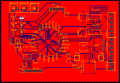
all parts excluding headers are SMD, and resistors/ capacitors are all package size 0805 (excluding the four electrolytic). the FPGA is a LCMX02. it uses two mx1508 motor drivers, which can control a total of four motors, but in this application only three are being used. for the 3.3v supply i am using a LM2596SX-3.3, using the provided schematic in the datasheet. because the spi control signal will be provided by an "arduino", i need a bi-directional logic shifter, and for this im using a TXS0108e. DATASHEET: http://www.ti.com/lit/ds/symlink/txs0108e.pdf. in the datasheet it says that when the OE input is high, data can be passed through. in my design am i doing this correctly?
another question i have is the power filtering/ decoupling section of the schematic. having no experience with this i used an example i found online. is this correct? do i need to use ferrite bead or the capacitors (x3) beforehand, or is the power from the regulator good enoughph? if i need the ferrite bead, what value should i use?
another question i have is about my inputs/ outputs. there are 6 leds (0805 smd), 3 potentiometer, and three switches. are the potentiometers/ other IO wired correctly?
my final question pertains to the motor drivers. in the schematic, the unused inputs/ grounds/ power are disconnected. do i need to do anything with these, or simply leaving them disconnected fine?
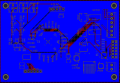
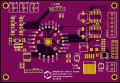
if anyone has any input on my design, or see any problems, please let me know. thanks! after i finish the schematic, i will start laying out the PCB.
EDIT: upon further thought, i probably need an ADC for the potentiometers. suggestions?
Disclaimer:
*the project requirements does not include creating a circuit. most/all are simply using the on-board IO on the basys3 development board.
*i am not asking for code, only schematic/ pcb help.
for my project i want to create something like this:
below is my schematic, but first i will describe it to the best of my ability. i want for the motor (12vdc) to spin at a speed set either by the on-board potentiometer or via SPI, whenever a switch is triggered (if you watch the video, the switch is on the arm), for a set amount of time. this will control a total of three spool holders (systems of 1x POT, 1x Switch, 1x Motor, 2x LED). led EN shows whether or not the POT is enabled or is under SPI control, and led TR shows whether the motor is triggered (active).
all parts excluding headers are SMD, and resistors/ capacitors are all package size 0805 (excluding the four electrolytic). the FPGA is a LCMX02. it uses two mx1508 motor drivers, which can control a total of four motors, but in this application only three are being used. for the 3.3v supply i am using a LM2596SX-3.3, using the provided schematic in the datasheet. because the spi control signal will be provided by an "arduino", i need a bi-directional logic shifter, and for this im using a TXS0108e. DATASHEET: http://www.ti.com/lit/ds/symlink/txs0108e.pdf. in the datasheet it says that when the OE input is high, data can be passed through. in my design am i doing this correctly?
another question i have is the power filtering/ decoupling section of the schematic. having no experience with this i used an example i found online. is this correct? do i need to use ferrite bead or the capacitors (x3) beforehand, or is the power from the regulator good enoughph? if i need the ferrite bead, what value should i use?
another question i have is about my inputs/ outputs. there are 6 leds (0805 smd), 3 potentiometer, and three switches. are the potentiometers/ other IO wired correctly?
my final question pertains to the motor drivers. in the schematic, the unused inputs/ grounds/ power are disconnected. do i need to do anything with these, or simply leaving them disconnected fine?
if anyone has any input on my design, or see any problems, please let me know. thanks! after i finish the schematic, i will start laying out the PCB.
EDIT: upon further thought, i probably need an ADC for the potentiometers. suggestions?
Last edited: