Facebook
 Google
 GitHub
 Linkedin
Hi guys,
I'm sure there is a better way of describing my circuit but I can't think on one at present.
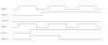
Brief
Two inputs, one delayed output!
scenario
Input 1 is triggered (lets say a 1 second pulse from 0 -> 5v -> 0)
this starts a 3 second timer
If input 2 is triggered within this time period then the output is enabled for 5 seconds.
Primary components
1 x 556 timer
1 x 4081 Quad AND gate
1x transistor of some sort to drive the relay
several resistors, a few capacitors and the odd diode for good measure!
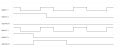
The theory being:
Trigger 1 goes into one input of a 556 timer that sets a 2 second pulse on the output which goes to an input of the AND gate
Trigger 2 goes to the other input of the AND gate
If both inputs are high, we get an output that goes to the second input of the 556 timer. The output of this timer is used to turn on a relay for 3 seconds.
Sorry for the really bad explanation but hopefully you get the gist.
Before I start on a circuit design I just wanted to find out if there is a far better solution to the one above.
Cheer, Philip
I'm sure there is a better way of describing my circuit but I can't think on one at present.
Brief
Two inputs, one delayed output!
scenario
Input 1 is triggered (lets say a 1 second pulse from 0 -> 5v -> 0)
this starts a 3 second timer
If input 2 is triggered within this time period then the output is enabled for 5 seconds.
Primary components
1 x 556 timer
1 x 4081 Quad AND gate
1x transistor of some sort to drive the relay
several resistors, a few capacitors and the odd diode for good measure!
The theory being:
Trigger 1 goes into one input of a 556 timer that sets a 2 second pulse on the output which goes to an input of the AND gate
Trigger 2 goes to the other input of the AND gate
If both inputs are high, we get an output that goes to the second input of the 556 timer. The output of this timer is used to turn on a relay for 3 seconds.
Sorry for the really bad explanation but hopefully you get the gist.
Before I start on a circuit design I just wanted to find out if there is a far better solution to the one above.
Cheer, Philip