Facebook
 Google
 GitHub
 Linkedin
panic mode
- Joined Oct 10, 2011
- 5,127
i think that is a nice but in the end it may be touchy.
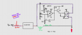
the first issue is that there is no delay. schematic shows a relay but really that is an SSR. and most significant delay will be the SSR turn-on time which is typically under 1ms. response of comparator is much shorter.
next, NTCs are not exactly the most stable or precise elements - quite the opposite. they have really high tolerances. also they have a wear and respond to other factors like temperature. for me that sounds as potentially perpetual concern and i would rather not have to periodically measure it, recalculate the circuit components and resolder parts.
the other issue is choice of zeners. not sure why they had to be so low (0.5 and 1V). zeners are notoriously inaccurate at low voltages and the lowest i recall is some 1.2V. at any rate, why not stick with something more common and more stable? as for Z2, i would only use it for IC input protection (10-15V). this would be handy in case NTC circuit connection becomes compromised or NTC fails open.
also switching large loads leads to transients and interference. there may be other circuits nearby that cause it too. i see nothing to deal with false triggers. and if it is pin3 trigger would latch the circuit so it would not perform what it was supposed to do. zener diodes have capacitance and since two different zeners are used, who is to tell which one will reach breakdown sooner? so it may be a good idea to add a capacitor in parallel with Z2. this can not only shift balance to the correct side, filter out possible transients but also create small delay... why not 3ms?
high current NTCs
https://www.vishay.com/docs/24512/mm.pdf
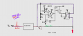