Buck converter based LED power supply

SgtWookie

Joined Jul 17, 2007
22,230
Had to make some changes. See the attached.

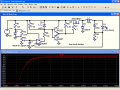
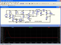
Zener is changed. Even that requires too much current. The LM2903 (same as LM393) output Vsat goes haywire when it tries to sink more than about 4.5mA.

Need a Zener with lower I(zt) rating. The one you used requires 49mA; that just won't work at all.

Had to change the grounding for C2; note that it's across the LED instead of directly to ground. If you try to ground it instead, the LED gets a high blast of current on startup.

I more than doubled the value of C2 and increased L1 to lower the ripple current through the LED.
 

Attachments

Last edited:

Wendy

Joined Mar 24, 2008
23,421
I question the location of C2. It will let the ripple flow through the cap to R8, and from there to the input of U1b. The current through the LED will be smoothed, which is good, but R8 will see no filtering from C2 at all. If anything the ripple will be dramatically increased to R8 because of it.

The attempt at wide voltage response is a major challenge. It is a lot simpler when you don't have such wide constraints. A lot of problems go away at the lower voltage ranges, such as 9VDC on the power supply. In the 9V-12VDC range currents aren't just a little bit lower throughout the circuit, the differences are major.

The dual emitter follower was a new one on me. I wonder how necessary R6 is, it is there to allow the gate to go to the Vcc voltage (and turn the MOSFET off).

Why is the gate resistor R7 so low?

I may have to find a new MOSFET, I just don't know about that one. This one is almost an ohm when turned on if I read the datasheet correctly.

Time to build a prototype and see what happens. Maybe the smoke will stay in the parts.
 

SgtWookie

Joined Jul 17, 2007
22,230
I question the location of C2. It will let the ripple flow through the cap to R8, and from there to the input of U1b. The current through the LED will be smoothed, which is good, but R8 will see no filtering from C2 at all. If anything the ripple will be dramatically increased to R8 because of it.
See the attached simulation. If C2 is grounded, you lose the soft start-up, and the LED gets blasted with ~4.4A. The initial charging of the cap requires a bunch of current, but if the cap is grounded, the feedback circuit is by voltage rather than current, and voltage feedback does not respond fast enough to prevent the overshoot. It's OK if Rsense (R8) has ripple on it. Where we don't want ripple is the LED.

The attempt at wide voltage response is a major challenge. It is a lot simpler when you don't have such wide constraints. A lot of problems go away at the lower voltage ranges, such as 9VDC on the power supply. In the 9V-12VDC range currents aren't just a little bit lower throughout the circuit, the differences are major.
Replacing certain resistors with constant current circuits would help that considerably.

The dual emitter follower was a new one on me. I wonder how necessary R6 is, it is there to allow the gate to go to the Vcc voltage (and turn the MOSFET off).
It's really optional. Why did you put it in? It would be OK for pulling the gate up if the emitter followers failed.

The way the circuit is now, the gate turn-on is really snappy, but turn-off is rather slow. This is due to the low Ib of of Q1, since Vcb will be very low, and R4 is rather large. Slow turn-off is not a big deal though; it's actually kind of helpful in this case, as it helps to avoid problems if there is inductance in the wiring from the power source to the source terminal. L1 is not allowed to saturate, so power dissipation in the MOSFET is low; average power dissipation is ~530mW.

Why is the gate resistor R7 so low?
The idea is to snub ringing on the MOSFET gate without delaying the charging/discharging of the gate by too much.

I may have to find a new MOSFET, I just don't know about that one. This one is almost an ohm when turned on if I read the datasheet correctly.
That VP2206N3 had worse specifications than any other P-ch MOSFET that I have available in LTSpice. Yes, it would turn on with Vgs=-5v, but I have no clue what Qg is (total gate charge) as it is not specified, and 900m is terrible for Rds(on).

If you used a parametric search engine like on Digikey or FairchildSemi, you'd start by looking for P-ch MOSFETS with a Vdss rating of 25v to 50v, and a low total gate charge - then decide the tradeoff between Rds(on) and Qg.

Actually, looking at the one I used in the simulation I realized that I ham-fingered my selection. Meant to use this one instead:
Si9803DY
Vdss=-25
Rds(on)=33m
Qg=15.8nC

The one shown actually has a Vdss of 20v, which is not sufficient for the simulation. In the real world, it would've gotten blasted any time it was turned off, as the difference between the source and drain would be Vcc+Vf(D2).

Time to build a prototype and see what happens. Maybe the smoke will stay in the parts.
Should work OK. If you use a 100uH inductor for L1 (like those that Radio Shack sells) your frequency should be around 60kHz when it stabilizes, and peak current will be within limits; those inductors are rated for 2A, and with R3 set to max output (~1A) the current in the inductor varies from ~.5A to ~1.5A each switching cycle. Keep in mind that 60kHz is the frequency that is used for WWBV, which is the time signal used by "atomic clocks", and that the 100uH inductors Radio Shack sells are wound on ferrite rod stock, which will result in broadcasting a 60kHz signal that will jam the WWBV in your local area. An inductor wound on a toroidal ferrite will reduce the emissions very significantly. If you discover that I'm correct about the frequency, please turn it off immediately.

You could slow the whole thing down by inserting a 1k resistor between the junction of R8/LED/cap and the noninverting input of the comparator, and a small cap from the comparator input to ground. Your current ripple will increase, but you can compensate for that by increasing C2.
 

Attachments

Wendy

Joined Mar 24, 2008
23,421
I'll keep an eye out for better LL p-channel MOSFETs, I had a sense the ones I have weren't too good. If they work however...

The soft start is a compelling argument. There is so little difference in the circuits I can modify the final design on the fly. I'm going to be drawing for a bit on this one, since I'm using a bread board as opposed to a protoboard.

If this works as hoped then we can use it as a standard for those folks who need a converter with their LEDs. The store bought brands are expensive. It may not be obvious on a CRT (the LCD monitors are really clearer, which is why I upgraded to a used 19") but your alias is attached to the schematic. You have a problem with that? If you don't it will be on the final print too.

We get a lot of posts asking about high power LEDs. It would be nice to offer something that wasn't a space heater as well as being a constant current source.
 
Last edited:

Thread Starter

tom66

Joined May 9, 2009
2,595
SgtWookie, where is the oscillator in that circuit?

I have built a SMPS without an oscillator before, but it is tricky to get it to start up. If it switches the transistor ON, but the current drops to zero before it reaches the peak current, the circuit will not oscillate. So you have to be very careful with the selection of inductor and capacitor in my experience. How have you solved this problem? I've been out of the loop for a while working on another project, so maybe I'm missing something...
 

SgtWookie

Joined Jul 17, 2007
22,230
I'll keep an eye out for better LL p-channel MOSFETs, I had a sense the ones I have weren't too good. If they work however...
Power dissipation in that MOSFET depends on how much current you're planning on putting through it. Might work for 20mA-100mA, but if you try for more, expect smoke - particularly with no heat sink. Note that the MOSFET I used has a Rds(on) of ~54m, a low gate charge, and average power dissipation of ~540mW. Your MOSFET has an Rds(on) nearly 17x as high; with 100mA current you'll be dissipating around 1W power.

The soft start is a compelling argument. There is so little difference in the circuits I can modify the final design on the fly.
It DOES seem like a very subtle change, doesn't it? However, you can see that it makes a vast difference in the startup.

Unless your new 'scope has a capture mode, you'll be hard-pressed to see it. Neither of my analog scopes has a capture mode, and I don't have a sound card interface built (yet). These LMC6484 could be good candidates. Those dual opamps you sent to me could be even better.

That reminds me, I picked up some CLC411 video amps awhile back (200MHz BW), I'll toss a couple of those in your package, too.

I'm going to be drawing for a bit on this one, since I'm using a bread board as opposed to a protoboard.
I'll recommend against breadboarding; there are just too many parasitics to deal with. Keep in mind that if the circuit is running at 40+kHz, you're dealing with square waves for the gate drive portion; to get a decent square wave you need far more BW than the fundamental frequency. An ideal square wave implies infinite bandwidth; as it is the sum of ALL of the odd harmonics.

Trying to build it on a breadboard is like starting off on a cross-country trip with a busted fan belt and a flat tire.

If this works as hoped then we can use it as a standard for those folks who need a converter with their LEDs. The store bought brands are expensive.
It's workable. There are fairly inexpensive ICs that only require a couple of supporting components (a cap and a resistor or two) but are somewhat difficult for hobbyists to use due to their small SMT/SMD packages.

We get a lot of posts asking about high power LEDs. It would be nice to offer something that wasn't a space heater as well as being a constant current source.
That's the idea. ;)
 
Last edited:

Wendy

Joined Mar 24, 2008
23,421
To me there is a major difference between breadboarding and protoboarding, and I suspect you meant the latter. It will take me about a week to get it done. Here is where I currently am. It is going to be tight.


I'm still puzzled how count_volta got his 2Hz oscillator to work using a protoboard. Good news for me though, I really was thinking of doing an article on it for the experiments section of the AAC book.
 

Attachments

Last edited:

SgtWookie

Joined Jul 17, 2007
22,230
SgtWookie, where is the oscillator in that circuit?
Basically, it's the inductor output coupled through C2 to the sense resistor R8 that causes the oscillation. The MOSFET gets turned off, the inductor current decays, and undershoots the reference voltage, causing the MOSFET to be switched back on. Basically, the circuit has too much gain to NOT oscillate.

I have built a SMPS without an oscillator before, but it is tricky to get it to start up. If it switches the transistor ON, but the current drops to zero before it reaches the peak current, the circuit will not oscillate. So you have to be very careful with the selection of inductor and capacitor in my experience. How have you solved this problem? I've been out of the loop for a while working on another project, so maybe I'm missing something...
Do you have LTSpice downloaded? You could experiment with the circuit if you'd like. Just download the attached .asc file to your LTSpice switchercad directory.
 

Attachments

Thread Starter

tom66

Joined May 9, 2009
2,595
Yeah, I have LTspice in a Windows XP virtual machine, so I'll give it a go. Are the inductor and capacitor critical to this design? My original idea was to create a generic supply which works with a 25mW signal LED all the way up to a 100W LED array; is this design capable of this?
 

SgtWookie

Joined Jul 17, 2007
22,230
To me there is a major difference between breadboarding and protoboarding, and I suspect you meant the latter.
There is a big difference.
Breadboards are generally white plastic (like a slice of white bread complete with holes), and you use jumper wires without solder to connect the components, power, and I/O signals.

Protoboards aka "prototype boards" aka "veroboard" aka "stripboard" are various types of fiberglass boards (FR-4 is most common) that usually are pre-drilled, most often on 0.1" centers, with copper on at least one side, in various patterns; from simply rows of "donuts" to solid strips of copper. Soldering is required for reliability.

Sometimes breadboards are mis-labeled or misidentified as prototype boards.

It sure would make things easier if everyone would agree on conventional nomenclature.

It will take me about a week to get it done. Here is where I currently am. It is going to be tight.

Don't be afraid to mount resistors/diodes vertically. Power dissipation will be quite low.

I'm still puzzled how count_volta got his 2Hz oscillator to work using a protoboard. Good news for me though, I really was thinking of doing an article on it for the experiments section of the AAC book.
Ahhh, he used a breadboard. ;) The load caps on the crystal slowed the edges enough. Once he minimized the length of wiring, he removed a lot of inductance (hence delays) from the circuit. Small gauge wire acts like delay lines due to the inductance.

Wide short traces act as infinite planes; an infinite plane has no inductance. (!)
That sentence is worth repeating:
Wide short traces act as infinite planes; an infinite plane has no inductance.

That is why designers use copper fill on PCBs for power and ground planes.
 

SgtWookie

Joined Jul 17, 2007
22,230
While a plane by itself has negligible inductance you will still have a loop area to connect into and out of the plane. Any loop area has inductance. That's why even with planes your runs are still kept as short as possible and you prefer to have tightly spaced layers.

http://www.daycounter.com/Calculators/Microstrip-Inductor-Calculator.phtml
We're in agreement. That's also why bypass caps should be sprinkled liberally around PCB's, particularly if the power rails or ground planes are interrupted/chopped up.

But, I'm digressing. The point I was trying to make is that you can virtually eliminate parasitic inductance (in the supply rails) by using copper-filled ground/power planes. Even with SMT/SMD devices, you're going to have some inductance in the leads - but it'll be a whole lot less than with DIP devices. For signals, short and wide traces will minimize the inductance, but parasitic capacitance can then wreak havoc if you have other planes parallel to the signal trace. Still, parasitic capacitance is a bit easier to deal with than parasitic inductance.
 

SgtWookie

Joined Jul 17, 2007
22,230
Yeah, I have LTspice in a Windows XP virtual machine, so I'll give it a go. Are the inductor and capacitor critical to this design?
Experiment, my friend. ;) Decreasing the size of the inductor will increase the ripple current in the load. Decreasing the size of C2 will increase the ripple current in the load.

Adding a filter stage consisting of a 4uH to 15uH inductor and a 100uF cap will help a great deal in eliminating ripple in the load; but for LEDs, this is not terribly important. As long as the average current is quite close with a high frequency, the power dissipation will remain the same, and the light output will be perceived as constant.

My original idea was to create a generic supply which works with a 25mW signal LED all the way up to a 100W LED array; is this design capable of this?
100 Watts of LEDs? Well, that's a bit ambitious.

Limiting factors are the comparator rails, the MOSFET Vdss/Id, diodes, etc. However, it could be used as a "building block" and repeated for parallel strings. Each string must have it's own current limiting.

Having 100W capability to use for a 25mW LED would simply not be realistic; the components would be excessively expensive. By the same token, what would you do if someone wanted to drive a 200W LED array using a 100W circuit?

It's not realistic to attempt to come up with a "one circuit fits all" solution for this, as it will be too expensive for many, and not capable enough for many others. However, the circuit as it is now can be "tuned" for operation in a range of nearly 0 current to around 1.2A current, and with the addition of a couple of components, operation over a lower or higher frequency range.
 

Ghar

Joined Mar 8, 2010
655
For these designs I guess L and C selection isn't that complicated but in general they do matter quite a bit.
They dominate the bandwidth of the system which determines what kind of transient response you can actually get with a control loop. For even faster transients you simply need a large C (or L) to hold the V (or I) constant before the loop responds.

When you shrink the inductor you tend to enlarge the capacitor due to higher ripple current requirements. When you decrease the capacitor you tend to increase the inductor to keep ripple down. If you keep both large your bandwidth becomes terrible and the output is very slow to respond to anything.

Make the inductor too small and you enter discontinuous conduction which completely changes the behaviour of the system.

There's a lot of compromises involved depending on the load, conversion ratio, and switching frequency but other things may come up as well.

@Wookie;
Agreed, I just got stuck on the phrase 'no inductance'
 

Thread Starter

tom66

Joined May 9, 2009
2,595
Sorry, I wasn't clear. 100 watts with the same circuit schematic. You'd have to spec in a much more powerful transistor for it to work, and possibly adjust the current shunt. The original schematic I posted (with the component values) is probably good up to 1-1.5 amp LEDs or about 4-5 watts. Perhaps more if active cooling is used and the transistor is properly heatsinked.
 

SgtWookie

Joined Jul 17, 2007
22,230
Sorry, I wasn't clear. 100 watts with the same circuit schematic.
As the circuit Bill and I are working on stands, it's limited to around roughly 1.2A due to Vref range vs R8 (Rsense). Changing the ratio of R2 to R3 would make it good for up to perhaps 6A; were L1 rated for 10A and C2 a low-ESR type and increased correspondingly in size to keep the ripple under control. Some damping/clamping on U1's noninverting input may become necessary.

You'd have to spec in a much more powerful transistor for it to work, and possibly adjust the current shunt. The original schematic I posted (with the component values) is probably good up to 1-1.5 amp LEDs or about 4-5 watts. Perhaps more if active cooling is used and the transistor is properly heatsinked.
Well, let's see - with Vcc @ 24v, you might get 22V @ 6A, so that would be 132W. That's if you had LEDs that could take 6A current. Average power dissipation in the MOSFET that I selected would be ~2W, but you'd still need a heat sink.
 
Last edited:

Thread Starter

tom66

Joined May 9, 2009
2,595
There hasn't been activity on this thread for two days so I thought I would submit an idea I had. I'm going to have to build this, but it's a much simpler design for SMPS, based on the MC34063A SMPS step-up/step-down/inverting controller IC.

This circuit takes advantage of the current limiting features of the IC. If Ipk is 300mV less than Vcc, it reduces the control signal. This is probably one of the simplest SMPS circuits for constant current limiting. Without external transistors the output current is probably no more than 300mA, which is good enough for 1W LEDs. The current has no actual upper bound (that is, you can tell it to output 10A by setting the dial at the bottom of the scale), but will be limited by the internal thermal dissipation of the chip (the chip will shut down if it overheats), and the output is clamped at 5V. It also implements soft start using a capacitor on Ipk, though this obviously slows the feedback loop down I don't see it being too much of a problem with LEDs which are relatively stable.

Any comments appreciated. I have a few MC34063A's, so I'm going to try and build this. I don't have any 15 ohm 2W resistors or power LEDs at the moment, but I'll try with 1/4w resistors and signal LEDs, as the 2W rating is only for high power LEDs (Pdis usually 0.6W at 300mA, but I'm overspecifying the resistors.)

The efficiency of this should be ~60% with low loads and 70-80% with high loads. Inductor and capacitor values were plucked out of thin air. Feel free to comment on my poor SMPS designing skills.
 

Attachments

SgtWookie

Joined Jul 17, 2007
22,230
Did you use ONsemi's Excel spreadsheet to calculate the values? If not, you should give it a try.

I'm not so hot on the MC33063/MC34063 series, as you lose about 1.3v via the internal Darlington switch. You really need to use an external switch to get decent efficiency out of it.

I think you've overestimated the efficiency you'll get. That 15 Ohm resistor is going to knock it down even further.
 

Thread Starter

tom66

Joined May 9, 2009
2,595
The values were calculated by the components I had. I don't have many inductors at the moment, they're one of the more pricey components for a hobbyist like me.

By the way, it didn't work. And I think I know why. Ipk is measured as a difference from Vcc, so it's difficult to control it. My circuit can adjust the Ipk voltage, but it brings it much further past 300mV differential, which leads the chip to try and put the maximum current through the LED... However, I have another idea using an external amplifier (probably a differential configuration of an op-amp) feeding a voltage into the COMP pin, so we'll see how it goes.

Good point on the efficiency, I didn't take into account the 0.6W wasted in the resistor; I was only reading the datasheet. So maybe 40% efficient. Not very good. This new version I mention will use a 0.01 ohm current shunt so will be much more efficient.

My reasons for the MC34063A: A) it's practically a jelly-bean part (TI make some, ONsemi make some, a few other companies as well) and there are lots of projects using it, so it's quite common; and B) I had some available, no other SMPS ICs at the moment.

Tom
 

SgtWookie

Joined Jul 17, 2007
22,230
Tom,
Have you seen Ronald Dekker's site?
http://www.dos4ever.com

He has a section called "Flyback Converters for Dummies". Don't let the title throw you. It's a really good intro to winding your own inductors and broadband transformers out of salvaged items.

The biggest hurdle is already over with if you have a decent oscilloscope. The "inductor test bench" is very simple and inexpensive to build.

The boost and flyback converter schematics can be built from very commonly available items. They won't be terribly efficient, but they will work, and give you some practical experience with the inductors you've wound.

Safety item: In both schematics, replace R4 with a 47k to 56k Ohm resistor; this limits the maximum output voltage to < 50v. This means that the neon bulb will not fire, so it can be omitted - or replaced with an LED and suitable current limiting resistor (say, 5.1k 1W for 10mA or 10k 500mW for 5mA).
 
Top