Facebook
 Google
 GitHub
 Linkedin
Hi everyone,
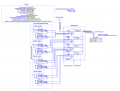
I am currently working on a 4-Phase Synchronous Buck Converter project. At this stage, my primary focus is verifying the core working principles and testing the interleaved phase control logic via simulation.
Note: My ultimate goal is to transition this simulation into a real, functional hardware prototype. Therefore, I am looking for practical hardware design and layout advice right from the start to avoid costly mistakes down the road.
The topology is hard-switching, designed for a wide input voltage range up to 60V. Here are the core specifications and simulation parameters I am currently using:
I am currently using a relatively low switching frequency of 30kHz per phase to keep hard-switching losses manageable. What is the typical frequency range used in modern industry applications for a buck converter at these voltage/current levels? I would love to hear some reference benchmarks for real-world designs.
For the inductors, I am planning to use standard toroidal/round ferrite core inductors. Given the 20A max continuous current per phase, these components will naturally be bulky. Because the current paths through the MOSFETs and inductors are continuous, thermal management is going to be a huge bottleneck on the physical board. Are there specific thermal dissipation strategies, layout tricks, or alternative magnetic core geometries I should consider at this scale?
To prevent one phase from hogging all the current on the physical PCB, I need to implement phase current balancing. I am also monitoring the total output current for system supervision.
Since this design will handle a massive 80A total at the output, if there are any crucial components, protection devices, grounding strategies (like separating Analog and Power GND), or copper thickness considerations that I have overlooked, please feel free to suggest them! I am still learning many facets of high-power hardware design and am fully open to your explanations on how these additions function and why they are necessary for a real board.


Attached is my current schematic and simulation file of LTSPICE (You can download it for detail) (For testing you can change your ouput by Vout_reg). Thank you in advance for your time and expertise!
I am currently working on a 4-Phase Synchronous Buck Converter project. At this stage, my primary focus is verifying the core working principles and testing the interleaved phase control logic via simulation.
Note: My ultimate goal is to transition this simulation into a real, functional hardware prototype. Therefore, I am looking for practical hardware design and layout advice right from the start to avoid costly mistakes down the road.
The topology is hard-switching, designed for a wide input voltage range up to 60V. Here are the core specifications and simulation parameters I am currently using:
- Input Voltage (V_in): Up to 60V (Wide input range)
- Output Voltage (V_out): 12V
- Target Output Current: 20A per phase (80A total continuous output)
- Switching Frequency (F_s): 30kHz per phase
- Dead Time (DT): 200ns
- Gate Drive Voltage (V_g): 12V
- Rise/Fall Time (T_rf): 100ns
- Phase Shift (T_s): Interleaved by 90degress (T_{per}/4)
I am currently using a relatively low switching frequency of 30kHz per phase to keep hard-switching losses manageable. What is the typical frequency range used in modern industry applications for a buck converter at these voltage/current levels? I would love to hear some reference benchmarks for real-world designs.
For the inductors, I am planning to use standard toroidal/round ferrite core inductors. Given the 20A max continuous current per phase, these components will naturally be bulky. Because the current paths through the MOSFETs and inductors are continuous, thermal management is going to be a huge bottleneck on the physical board. Are there specific thermal dissipation strategies, layout tricks, or alternative magnetic core geometries I should consider at this scale?
To prevent one phase from hogging all the current on the physical PCB, I need to implement phase current balancing. I am also monitoring the total output current for system supervision.
- I intend to use DCR sensing (sampling across the inductor using an RC network).
- Could anyone guide me on the correct methodology for calculating the R and C values relative to the inductor's DCR and L?
- Furthermore, since this signal needs to be fed back to an MCU with a 3.3V analog input limit, what are the best filtering, scaling, or overvoltage clamping practices to read this signal accurately without damaging the MCU?
Since this design will handle a massive 80A total at the output, if there are any crucial components, protection devices, grounding strategies (like separating Analog and Power GND), or copper thickness considerations that I have overlooked, please feel free to suggest them! I am still learning many facets of high-power hardware design and am fully open to your explanations on how these additions function and why they are necessary for a real board.
Attached is my current schematic and simulation file of LTSPICE (You can download it for detail) (For testing you can change your ouput by Vout_reg). Thank you in advance for your time and expertise!
Attachments
-
 71.8 KB Views: 6
 -
 246.6 KB Views: 6
 -
33.9 KB Views: 3