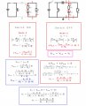
Would it help if we went through the analysis step by step ?
Since you dont seem to have a problem with the averaging techniques, maybe it would help to take one step back and do some regular analysis that produces the equations just before the averaging.
We could even start with a regular resistor and capacitor being charged and discharged by a pulsing source similar to the converter with duty cycle D as before, then add a little complexity and redo the analysis like by adding an inductor or another capacitor and resistor.
Would it help if we went through the analysis step by step ?
Since you dont seem to have a problem with the averaging techniques, maybe it would help to take one step back and do some regular analysis that produces the equations just before the averaging.
We could even start with a regular resistor and capacitor being charged and discharged by a pulsing source similar to the converter with duty cycle D as before, then add a little complexity and redo the analysis like by adding an inductor or another capacitor and resistor.
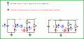
Do you understand why ALL the arrows are drawn the way they are, in the direction they are?
That's really the first step. (BTW the last arrow on the right can be taken to be i=Vo/R of course).
Do you understand why ALL the arrows are drawn the way they are, in the direction they are?
That's really the first step. (BTW the last arrow on the right can be taken to be i=Vo/R of course).
No, I don't really know why is it, maybe it's something methodically, so we don't have to change directions presupposing things. Could you explain me please?
No, I don't really know why is it, maybe it's something methodically, so we don't have to change directions presupposing things. Could you explain me please?
Yes it is partly methodical, in that everything 'higher up' in the drawing is assumed to be more positive, while everything 'lower' in the drawing is assumed to be negative. It helps to keep everything the same throughout multiple drawings and this would be especially true when making two drawings of the same circuit like we do here where one drawing is for one mode and the other drawing is for the other mode. This is also true when applying principles like superposition and i think you could guess why. For example, we would not want to show the source "E" (Vin) as positive on top in one drawing and show it as having positive on the bottom on the next drawing. Not only will that most likely not work, there is no good reason to try to do that.
I hope you can appreciate this view because i think it will help you.
Piecewise however, we are using the idea of conventional current so for a two terminal element with current entering on say the top terminal that must be the most positive node symbolically, regardless how the numerical solution comes out later. So for resistors, capacitors, etc., if the element is drawn vertically and the current flows DOWN in the element then the top terminal must be the most positive. This is really mandatory.
Finally, in a circuit where we have two modes such as the circuit we have been working with, the final equations must incorporate both modes and so reversing a current or voltage in one mode and not the other is going to lead to a sign change which cant be right.
To abbreviate a little, the two ODE's came out in the form:
L*i=f1(i,v)
C*v=f2(i,v)
and:
L*i=f3(i,v)
C*v=f4(i,v)
but if we allow a change in the direction of current in only the second set then we might end up with:
L*i=f1(i,v)
C*v=f2(i,v)
and:
L*i=f3(i,v)
C*v=-f4(i,v)
which is not the same set of equations and so probably will not work out correctly.
So it is much better to keep the directions of currents and voltage the same in BOTH circuit modes. This alone could be the source of your problem in developing the required equations.
Yes it is partly methodical, in that everything 'higher up' in the drawing is assumed to be more positive, while everything 'lower' in the drawing is assumed to be negative. It helps to keep everything the same throughout multiple drawings and this would be especially true when making two drawings of the same circuit like we do here where one drawing is for one mode and the other drawing is for the other mode. This is also true when applying principles like superposition and i think you could guess why. For example, we would not want to show the source "E" (Vin) as positive on top in one drawing and show it as having positive on the bottom on the next drawing. Not only will that most likely not work, there is no good reason to try to do that.
I hope you can appreciate this view because i think it will help you.
Piecewise however, we are using the idea of conventional current so for a two terminal element with current entering on say the top terminal that must be the most positive node symbolically, regardless how the numerical solution comes out later. So for resistors, capacitors, etc., if the element is drawn vertically and the current flows DOWN in the element then the top terminal must be the most positive. This is really mandatory.
Finally, in a circuit where we have two modes such as the circuit we have been working with, the final equations must incorporate both modes and so reversing a current or voltage in one mode and not the other is going to lead to a sign change which cant be right.
To abbreviate a little, the two ODE's came out in the form:
L*i=f1(i,v)
C*v=f2(i,v)
and:
L*i=f3(i,v)
C*v=f4(i,v)
but if we allow a change in the direction of current in only the second set then we might end up with:
L*i=f1(i,v)
C*v=f2(i,v)
and:
L*i=f3(i,v)
C*v=-f4(i,v)
which is not the same set of equations and so probably will not work out correctly.
So it is much better to keep the directions of currents and voltage the same in BOTH circuit modes. This alone could be the source of your problem in developing the required equations.
Hi !
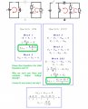
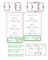
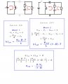
I've Already tried to do, and it didn't work. Actually, the problem I see, it's that I had the same equations as you, but you did some extra steps that looked tangled to me, and I still don't know why we couldn't use directly the both inductor current increments equations, and you said something about not to avoid steps, but i was look correct to do it, just the solution was not correct. I will post now the procedure remaining the same direction of the currents.
Hi !
I've Already tried to do, and it didn't work. Actually, the problem I see, it's that I had the same equations as you, but you did some extra steps that looked tangled to me, and I still don't know why we couldn't use directly the both inductor current increments equations, and you said something about not to avoid steps, but i was look correct to do it, just the solution was not correct. I will post now the procedure remaining the same direction of the currents.
Well sometimes you just have to sit down and roll your sleeves up and dig down into it. This sometimes means you will have to experiment until you get the right result. If you think that changing the direction of one of the currents is the problem, then reverse it and try again. Since you said you use Maxima this should not be too bad to repeat just to see if you get a better result.
I still have a question though about your last equation:
iL=-Vo/(R*(1-D))
What do you intend to use for "Vo", and so what is your NUMERICAL result for iL given:
R=10
D=0.5 (50 percent duty cycle)
and some other values:
L=1
C=1
Rc=0.1
?
Also, i thought you wanted to get the solution for the two sets of ODE's too, because that is a somewhat canonical form used in many published papers and with slight modification is exactly in a canonical form.
Well sometimes you just have to sit down and roll your sleeves up and dig down into it. This sometimes means you will have to experiment until you get the right result. If you think that changing the direction of one of the currents is the problem, then reverse it and try again. Since you said you use Maxima this should not be too bad to repeat just to see if you get a better result.
That was not about experimenting, that was a huge lack of understanding of how this kind of circuits works, and what assumptions we are doing in order to solve the circuit.
Since I started college again, I asked to my classmates if they know how to solve this circuits adding the ESR, and one of them said that I had a misunderstanding about what assumptions we are actually doing, like current in the inductor must be linear so we can assume that mean current value is the same in both ON and OFF states and same to the Cap Voltage. Then, when we add the inner resistance to the Cap, the Output Voltage (Vo) it's no longer the same average voltage in both states ON and OFF, so Output Voltage (Vo) must to be differentiated as Vo-on and Vo-off.
Then the whole period Vo mean voltage, I found experimenting, that it's the same as Cap mean Voltage (Vc), and
Vo = Vo-on · D + Vo-off · (1-D) , works too, I actually don't know why works both of them.

 Facebook
 Google
 GitHub
 Linkedin