Facebook
 Google
 GitHub
 Linkedin
I would be the first to say this is a case where it is easier and cheaper to buy a commercial inverter. It is hard to beat a design that has been professionally designed and built with safety and specs in mind. However, we've been getting a lot of this schematic.
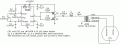
http://www.tonyvanroon.com/oldwebsite/circ/555dcac.html

..................................................................Figure 1
This circuit bugs me. It has so many flaws that I'm not going to bother going over them in this paragraph, except many of the posts at All About Circuits sum up to "Why doesn't this work?". It doesn't help it was stolen and posted here. I'll post several ideas that will work to various degrees and discuss their advantages and disadvantages, with the proviso that the first paragraph states how I feel about this subject. I am writing this to give folks at AAC a place to point the many inverter requests we have gotten over the long haul.
Feel free to trash my ideas as I come up with them. If I like the criticism I will add it to the tutorial. This is both a how to and why you shouldn't kinda article. I would not use a home made inverter normally, it would take a major disaster such a plague or meteor strike to make me do it. Therefore, I am not responsible for any of the circuits I am about to present or your use of them! If you use this article, you do so at your own risk!
Another common theme from posters is a lack of real understanding of waveforms, frequency, RMS, P-P, and power. All of these are critical, so I will go through them.
It is also important to understand AC wiring. These vary from country to country, both in power specs and safety specs. I will assume the US standards, 120VAC 60Hz with a ground. The ground requirement is fairly universal as far as I know, so I will show how to do it on a portable inverter. It is up to the builder to make it safe. Voltages and currents in these ranges are LETHAL! Please do not take shortcuts as far as the AC output is concerned. Build them as close to code as you can.
Now for the first schematic:

........................................................Figure 2
This schematic is old, when I started studying electronics over 30 years ago it was around. It has big problems with voltage output stability, frequency stability, duty cycle, and in producing a square wave. While it might work on a large number of applications the only thing I would trust it with is light bulbs. When I first drew it I used single transistors, but after a little reflection I realized they would not have enough gain, so I switched them off for Darlington Pairs, which come in prepackaged formats. Something like a TIP-100 or an equivalent would work for this. They will get quite hot, so heat sink them properly. They will also cause about 12 V drop on the AC output compared to conventional single transistors. The actual output voltage is dependent on both the components and the power supply voltage.
The frequency output is only an approximation, if you need to tweak them add two identical resistors in series with R1 and R2 (one for each resistor) to drop the frequency. Conventional power diodes (such as the 1N4001) will work for all the diodes. Do not use resistors lower than 120Ω, as they will get much hotter and possibly burn up. Use 150Ω for R1 and R2 for 50Hz.
You may run into the problem of "flux walking". This happens when the duty cycles of the two transistors are not exactly the same. Current flow is imbalanced, and the transformer core saturates. This causes extremely high current flow in the transistors, resulting in smoke.
The Figure 3 is based off of Figure 1, but it has been cleaned up as much as I was able. I left L1 to minimize the RF interference produced by the square wave. It will not help much, but it is better than nothing. Neither Figure 1 or Figure 3 will produce much power. If you get 10 watts out of either designs I would be surprised. Figure 1 has no protections for the transistors, either they or the transformer will blow if pushed beyond their limits. Figure 1 also looses more than 2.4VDC with all the BE drops (over 20% of the drive voltage), which my design corrects. C4 is another source of loss, it is 1Ω at 60Hz and 1.2Ω at 50Hz, but while it adds to the loss it is necessary. It will loose 24 volts of the AC output for a max of 96 VAC out, when C4 is taken into account it is even more. The symmetry was a bit further off than I liked too (just over 52%), so I tweaked it to around 50.2%. Basically both are little more than science fair projects, showing how it is done without being able to do much.

.......................................................................................Figure 3
So far we have used BJT type transistors. They are common, they are cheap, but they have problems with high power. They generally use 10% of the Collector current for the Base. It you have 10 amps through the collector (which will light a light bulb) you will have 1A going though the base. This is a limiter for how much current you have going through the transformer, as well as being very wasteful and generates extra heat. Technology has solved this problem in the form of a MOSFET.
MOSFETs are voltage controlled devices, and when they are on they have very low resistances. Their only drawback is they take a substantial amount of current to force the gate to change in the form of a surge. The gate looks like a capacitor, after it is charged it takes almost no current to keep it there, for all intents and purposes no current. I have substituted the 555 with a CMOS 555 because a CMOS 555 will go rail to rail, unlike a conventional 555.

.......................................................................................Figure 4
Generally Push Pull outputs like these have to have something to prevent shoot through, a condition where both transistors Q1 and Q2 are on at the same time during a transition. If this happens long enough one or both the transistors may fry, a bad thing. Figure 3 uses the zeners to allow one transistor turn off before the other turns on, with this design (Figure 4) the inductors L2 and L3 slow Q1 and Q2 turning on while the other turns off.
http://www.tonyvanroon.com/oldwebsite/circ/555dcac.html
..................................................................Figure 1
This circuit bugs me. It has so many flaws that I'm not going to bother going over them in this paragraph, except many of the posts at All About Circuits sum up to "Why doesn't this work?". It doesn't help it was stolen and posted here. I'll post several ideas that will work to various degrees and discuss their advantages and disadvantages, with the proviso that the first paragraph states how I feel about this subject. I am writing this to give folks at AAC a place to point the many inverter requests we have gotten over the long haul.
Feel free to trash my ideas as I come up with them. If I like the criticism I will add it to the tutorial. This is both a how to and why you shouldn't kinda article. I would not use a home made inverter normally, it would take a major disaster such a plague or meteor strike to make me do it. Therefore, I am not responsible for any of the circuits I am about to present or your use of them! If you use this article, you do so at your own risk!
Another common theme from posters is a lack of real understanding of waveforms, frequency, RMS, P-P, and power. All of these are critical, so I will go through them.
- Waveforms - Most simple switching circuits generate square waves. The signal sent to you from the power company is a sine wave. Sine waves are pure, they do not generate much in the way of RF, while square waves aren't, and can spatter the spectrum. If you have a piece of equipment that uses RF (stereos, TVs, satellite receivers, any wireless gear) this can be a real nuisance. It also has major ramifications in voltages, which will be discussed in the RMS and P-P paragraph.
- Frequency - We take the AC delivered by the power company for granted, but they pay close attention to the accuracy of the frequency of their power. In many cases they count the number of cycles in a day, and subtly adjust the frequency to make it come out right. This is because many pieces of equipment, such as digital clocks, use this as their time bases. Back in the days of TVs using tubes it was also used to make the internal oscillators of the TV stay on track, as this simplified the circuits considerably.
- RMS - This is the amount of real power (how much heat a resistor dissipates) a waveform will deliver. It the case of a sine wave the power is X 0.707 the peak value of the wave form. In the case of a square wave it is X 1 the value. Problem is, many power supply circuits use the peak value, so while a square wave may deliver the same amount of power you may be feeding a piece of equipment some seriously wrong voltages. To make it worse, a digital volt meter (DVM) or a volt ohm meter (VOM) will not be able to tell the difference on the AC scale!
- P-P - This closely related to RMS. Many people confuse Peak to Peak with RMS. Generally P-P is dictated by the battery voltage. Another number, the peak voltage, is ½ the P-P value.
- Power - The power delivered by an inverter is the same as the power input by the inverter, plus losses. Losses are a fact of life, they don't go away. If a circuit has a 20% loss it is probably doing pretty good. So lets say you want to power a 120W light bulb at 120VAC. This means the bulb will use 1 amp (I = P / V). If you have a 12V power supply, and it is feeding a 120W, then you are taking in 144W (remember the 20% loss?). This means your battery is providing 12 Amps! It only gets worse as the wattages go up. Battery current is a common problem with all inverters. There is also the fact the more amperage you want the larger and more expensive the transformer needs to be.
It is also important to understand AC wiring. These vary from country to country, both in power specs and safety specs. I will assume the US standards, 120VAC 60Hz with a ground. The ground requirement is fairly universal as far as I know, so I will show how to do it on a portable inverter. It is up to the builder to make it safe. Voltages and currents in these ranges are LETHAL! Please do not take shortcuts as far as the AC output is concerned. Build them as close to code as you can.
Now for the first schematic:
........................................................Figure 2
This schematic is old, when I started studying electronics over 30 years ago it was around. It has big problems with voltage output stability, frequency stability, duty cycle, and in producing a square wave. While it might work on a large number of applications the only thing I would trust it with is light bulbs. When I first drew it I used single transistors, but after a little reflection I realized they would not have enough gain, so I switched them off for Darlington Pairs, which come in prepackaged formats. Something like a TIP-100 or an equivalent would work for this. They will get quite hot, so heat sink them properly. They will also cause about 12 V drop on the AC output compared to conventional single transistors. The actual output voltage is dependent on both the components and the power supply voltage.
The frequency output is only an approximation, if you need to tweak them add two identical resistors in series with R1 and R2 (one for each resistor) to drop the frequency. Conventional power diodes (such as the 1N4001) will work for all the diodes. Do not use resistors lower than 120Ω, as they will get much hotter and possibly burn up. Use 150Ω for R1 and R2 for 50Hz.
You may run into the problem of "flux walking". This happens when the duty cycles of the two transistors are not exactly the same. Current flow is imbalanced, and the transformer core saturates. This causes extremely high current flow in the transistors, resulting in smoke.
The Figure 3 is based off of Figure 1, but it has been cleaned up as much as I was able. I left L1 to minimize the RF interference produced by the square wave. It will not help much, but it is better than nothing. Neither Figure 1 or Figure 3 will produce much power. If you get 10 watts out of either designs I would be surprised. Figure 1 has no protections for the transistors, either they or the transformer will blow if pushed beyond their limits. Figure 1 also looses more than 2.4VDC with all the BE drops (over 20% of the drive voltage), which my design corrects. C4 is another source of loss, it is 1Ω at 60Hz and 1.2Ω at 50Hz, but while it adds to the loss it is necessary. It will loose 24 volts of the AC output for a max of 96 VAC out, when C4 is taken into account it is even more. The symmetry was a bit further off than I liked too (just over 52%), so I tweaked it to around 50.2%. Basically both are little more than science fair projects, showing how it is done without being able to do much.
.......................................................................................Figure 3
So far we have used BJT type transistors. They are common, they are cheap, but they have problems with high power. They generally use 10% of the Collector current for the Base. It you have 10 amps through the collector (which will light a light bulb) you will have 1A going though the base. This is a limiter for how much current you have going through the transformer, as well as being very wasteful and generates extra heat. Technology has solved this problem in the form of a MOSFET.
MOSFETs are voltage controlled devices, and when they are on they have very low resistances. Their only drawback is they take a substantial amount of current to force the gate to change in the form of a surge. The gate looks like a capacitor, after it is charged it takes almost no current to keep it there, for all intents and purposes no current. I have substituted the 555 with a CMOS 555 because a CMOS 555 will go rail to rail, unlike a conventional 555.
.......................................................................................Figure 4
Generally Push Pull outputs like these have to have something to prevent shoot through, a condition where both transistors Q1 and Q2 are on at the same time during a transition. If this happens long enough one or both the transistors may fry, a bad thing. Figure 3 uses the zeners to allow one transistor turn off before the other turns on, with this design (Figure 4) the inductors L2 and L3 slow Q1 and Q2 turning on while the other turns off.

")